Light-emitting photonic device

a photonic device and light-emitting technology, applied in semiconductor lasers, lighting and heating equipment, instruments, etc., can solve the problems of increasing manufacturing costs and equipment size, increasing device size, power consumption, and product quality, and reducing the lifetime and reliability of light sources. , to achieve the effect of minimizing crosstalk and avoiding crosstalk

Inactive Publication Date: 2010-08-10
CANON KK
View PDF37 Cites 14 Cited by
  • Summary
  • Abstract
  • Description
  • Claims
  • Application Information

AI Technical Summary

Benefits of technology

[0040]According to one aspect of the invention, a colored light source apparatus is provided. The apparatus includes light sources corresponding to active regions defined by defects in a photonic crystal structure, wherein the photonic crystal structure is based on periodic structures. The apparatus also includes a waveguide, a first electrode, and a second electrode. Varying electrical properties between the first and second electrodes stimulates radiation production in the active regions, wherein the radiation is at least partially coupled to and guided by the waveguide.
[0048]The light sources can include at least a first light source, a second light source and a third light source, wherein the first light source emits stimulated radiation of a first frequency, the second light source emits stimulated radiation of a second frequency, and the third light source emits stimulated radiation of a third frequency, and wherein the first, second and third light sources are arranged according to their respective emitted frequencies so that the distance between any two of the first, second and third light sources can be minimized while minimizing crosstalk between the any two light sources.

Problems solved by technology

The generated heat not only reduces the lifetime and reliability of the light sources, but also results in bulky and power consuming thermal dissipation mechanisms and components, which increase the size, power consumption, and production costs of devices.
In many free space imaging systems, incoherent light sources are preferred over coherent light sources, since coherent light sources may introduce unintended interference artifacts, such as speckles.
In addition, coherent light sources require additional components such as diffusers, typically leading to increased manufacturing costs and equipment size.
However, such lamps have several technological limitations.
First, these lamps typically have low wall-plug efficiencies.
Moreover, since they are white light sources, the mechanisms to filter out RGB (red-green-blue) lights respectively and to dump useless IR (infrared) and UV (ultraviolet) components further reduce the net wall-plug efficiency.
This low efficiency not only consumes more power directly, but also generates additional heat, requiring additional components to dissipate the heat.
These thermal dissipation components (such as electrical fans and TEC (thermal electrical coolers, or Peltier coolers, with a description available at http: / / www.digit-life.com / articles / peltiercoolers / )) add cost, size, and power consumptions to the total system.
Moreover, the fabrication cost for LEDs is usually lower than that of laser diodes.
However, it should be noted that some laser diode arrangements are undesirable.
These extra steps typically result in a significantly more complex device structure (high fabrication cost and larger device size) and lower wall-plug efficiencies.
Such power levels cannot typically be provided by existing microcavity laser designs, such as VCSELs (Vertical Cavity Surface Emitting Lasers).
However, such sophisticated systems are expensive to produce.
For this reason, such lasers have not yet found their positions in the competitive consumer product markets of data projectors and LBPs.
However, such external optical lens systems (or extern diffraction systems) increase the size and cost of the light source.
In addition, such systems have problems related to the free space alignment packaging costs, and the alignment stability susceptible operation environment.
However, such a system will likely not function stably.
Such cross-talk between lasers will simply tend to phase lock the lasers into an undesirable low loss supermode.
An optical feedback and cross-talk system with multiple laser cavities and waveguides may support multiple supermodes with quality factors within the >20 nm gain bandwidth of the quantum wells, but such a system is likely to be unstable.
As such, delivering large optical power through the small waveguide cross-section is likely to result in device overheating and nonlinear optical effects caused by high optical power density.

Method used


Image

  • Light-emitting photonic device
  • Light-emitting photonic device
  • Light-emitting photonic device

Examples


Embodiment Construction

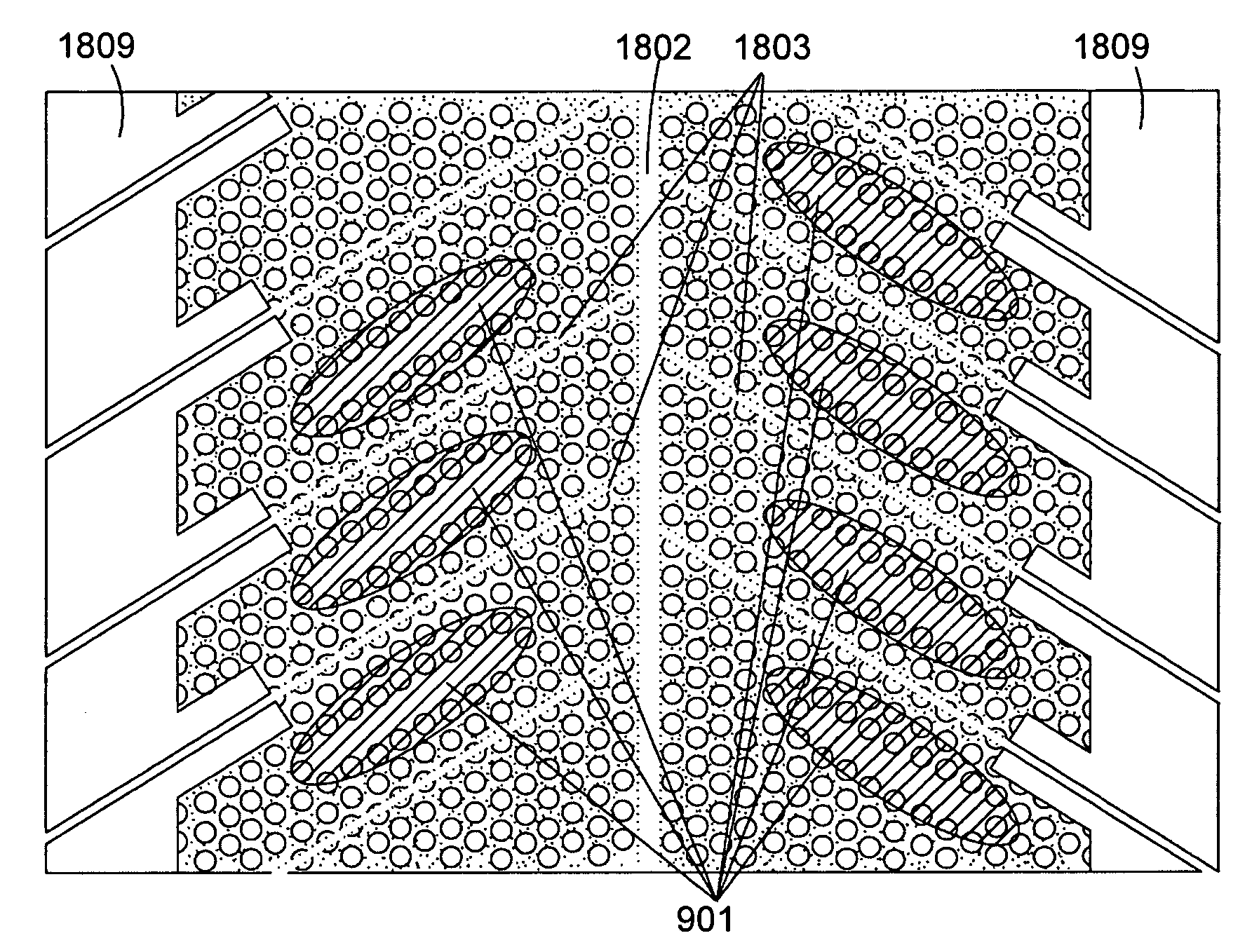
[0104]Referring to FIG. 5, the embedding of an array of photonic crystal light sources (or microcavities) in a media of photonic crystal is shown. The array of single mode photonic crystal light sources is also coupled into a common waveguide to generate output.

[0105]The concept of non-cross-talk optical power collection system can be achieved by forming the array of microcavities to resonate at different wavelengths. By doing so, each individual microcavity will naturally reject any optical power at different wavelengths (i.e. from a different microcavity).

[0106]As seen in FIG. 5, the coupling bandwidth from each mode to the common waveguide is smaller than the wavelength spacing between any two light sources in the array. Therefore, there is virtually no cross-talk between any two light sources in the array through the waveguide. Such a natural optical isolation mechanism can be demonstrated by numerical simulation, such as by FDTD (finite-difference time-domain) simulation. For i...


PUM


Abstract

A colored light source apparatus is provided. The apparatus includes light sources corresponding to active regions defined by defects in a photonic crystal structure, wherein the photonic crystal structure is based on periodic structures. The apparatus also includes a waveguide, a first electrode, and a second electrode. Varying electrical properties between the first and second electrodes stimulates radiation production in the active regions, wherein the radiation is at least partially coupled to and guided by the waveguide.

Description

CROSS-REFERENCE TO RELATED APPLICATION[0001]This application claims the benefit of U.S. Provisional Patent Application No. 60 / 628,601 filed Nov. 16, 2004, the contents of which are hereby incorporated by reference as if fully stated herein.BACKGROUND[0002]1. Field of the Invention[0003]The present invention is generally directed to colored light sources, and more particularly, although not exclusively, to colored light sources used in projectors and / or printers.[0004]2. Description of the Related Art[0005]Colored light sources have been used in different devices. For example, colored light sources have been used in data projectors and in polygon mirror scanning laser beam printers (LBPs).[0006]FIGS. 1 to 3 depict the structure of typical colored data projectors. In FIG. 1, the structure and the light source in a typical DMD (Digital Micromirror Device) based color wheel color-projection system, which can also be referred to as a DLP™ (Digital Light Processing™) system, are shown. Th...

Claims


Application Information

Patent Timeline
Patent Type & Authority Patents(United States)
IPC IPC(8): H01L33/00
CPCB82Y20/00G02B6/12007G02B6/1225H01S5/026H01S5/2232H01S5/4031H01S5/405H04N9/3129H01S5/0422H01S5/0425H01S5/105H01S5/2059H01S5/221H01S5/2214H01S5/3211H01S5/34306H01S5/34373H01S5/4087H01S5/04254H01S5/04256H01S5/04257H01S5/11
Inventor CAO, JIANG-RONGMIYAWAKI, MAMORU
Owner CANON KK
Why Eureka
Try Eureka