Adjacent plated through holes with staggered couplings for crosstalk reduction in high speed printed circuit boards

a technology of parallel plated through holes and printed circuit boards, applied in the field of signaling systems, can solve the problems of system integrity suffer, risetime of data transition from a zero to a one becoming faster, coupling between two signal conductors, etc., and achieve the effect of minimizing crosstalk between adjacent traces

Inactive Publication Date: 2011-08-16
AMPHENOL CORP
View PDF53 Cites 13 Cited by
  • Summary
  • Abstract
  • Description
  • Claims
  • Application Information

AI Technical Summary

Benefits of technology

[0010]Accordingly, it is one object of the invention to provide an electrical signal connection, an electrical signaling system, and a method of connecting that minimizes crosstalk between adjacent traces.

Problems solved by technology

However, system integrity suffers as the risetime of data transitioning from a zero to a one becomes faster.
One often encountered problem is coupling between two signal conductors.
However, direct electromagnetic coupling between adjacent via pairs will occur and result more severe crosstalk levels.
A major disadvantage is that it exponentially reduces the number of available routing pairs in a printed circuit board.
To recover the lost routing pairs, the number of signal layers is increased or the area of the printed circuit board panel is increased, resulting in greater overall cost of the printed circuit board.
Higher costs may be unacceptable in cost sensitive systems.
However, one disadvantage is that it is not possible to ideally route all adjacent pairs near the surface of the printed circuit board as the routing space in the layers close the surface are limited.
Further, connecting only near the surface provides fewer connection points so that reducing crosstalk by alternating assignments to ground, the method described above, is not feasible.

Method used


Image

  • Adjacent plated through holes with staggered couplings for crosstalk reduction in high speed printed circuit boards
  • Adjacent plated through holes with staggered couplings for crosstalk reduction in high speed printed circuit boards
  • Adjacent plated through holes with staggered couplings for crosstalk reduction in high speed printed circuit boards

Examples


Embodiment Construction

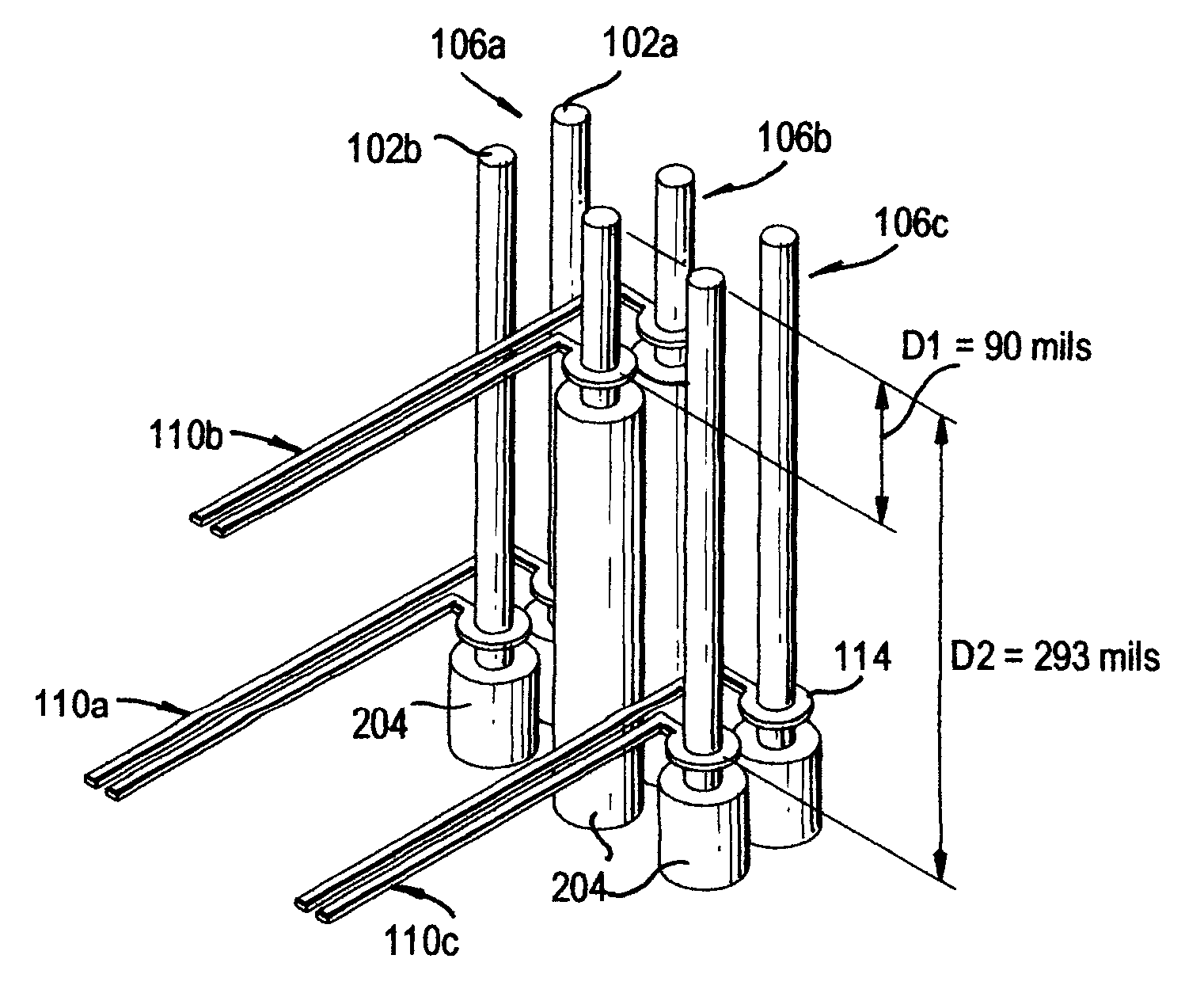
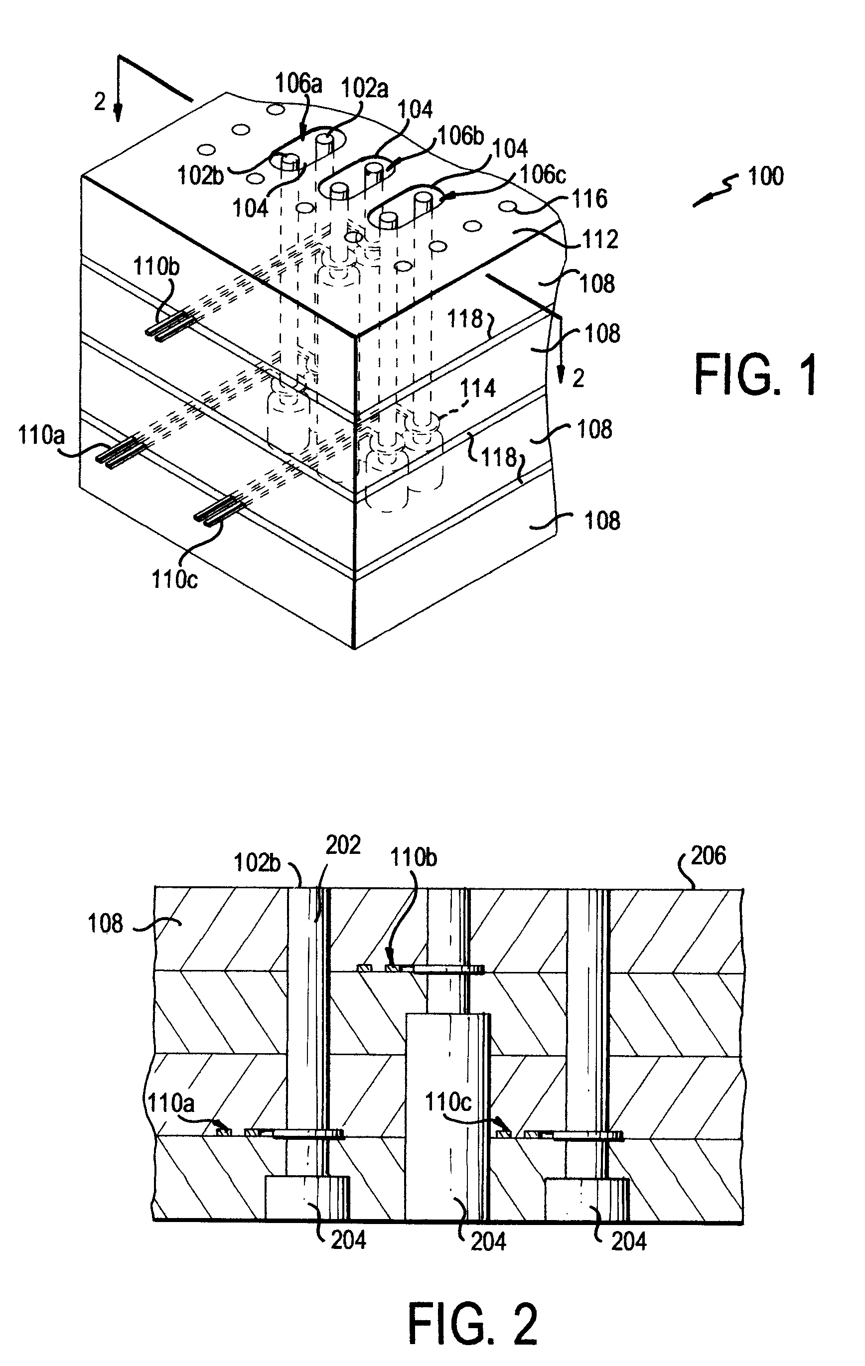
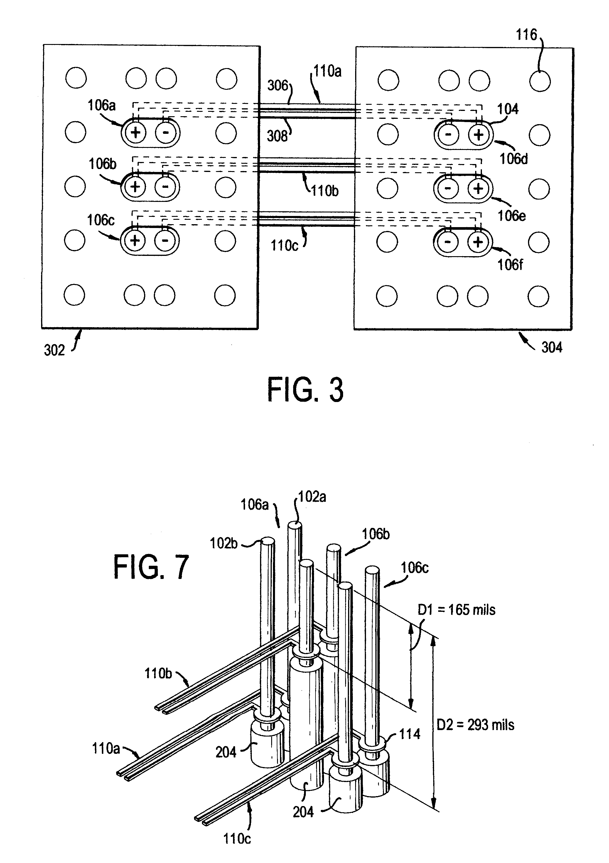
[0026]Referring to FIGS. 1-10, the present invention relates to an electrical signal connection that minimizes electromagnetic coupling or crosstalk between adjacent traces 110a-110c. Minimizing crosstalk decreases the distortions in signals transmitted by adjacent traces 110a-110c. Crosstalk is minimized by locating adjacent traces 110a-110c on different layers 108 of a printed circuit board 100. A distance between the adjacent traces 110a-110c is configured to minimize crosstalk of a certain frequency. As the distance is decreased, a higher frequency of crosstalk is minimized, and in a similar fashion, a larger distance results in minimizing crosstalk of a lower frequency. Also, if the distance between adjacent traces 110a-110c is configured for a particular frequency and the distance is maintained between adjacent traces 110a-110c, the adjacent traces 110a-110c can be located on any layer 108 and still minimize the crosstalk for that particular frequency.

[0027]Referring to FIG. 1...


PUM


Abstract

An electrical signal connection, an electrical signaling system, and a method of connecting printed circuit boards. The electrical signal connection having a first conductive via and a second conductive via disposed in a first printed circuit board. A first conductive trace with a first end and a second end has the first end electrically coupled to the first conductive via at a first distance from the top surface of the first printed circuit board. The second end of the first conductive via is electrically coupled to the second printed circuit board. A second conductive trace with a first end and a second end has the first end being electrically coupled to the second conductive via at a second distance from the top surface of the first printed circuit board. The second end being is electrically coupled to the second printed circuit board.

Description

FIELD OF THE INVENTION[0001]The present invention relates generally to the field of signaling systems for transmitting information over wires with connectors for printed circuit boards. In particular, the present invention relates to a signaling system in which traces are used to connect printed circuit boards and crosstalk is minimized between adjacent traces.BACKGROUND OF THE INVENTION[0002]The proliferation of many new high-speed digital standards is increasingly testing the limits of transmitting a signal. Data must be transmitted with very few bit errors to maintain system reliability. However, system integrity suffers as the risetime of data transitioning from a zero to a one becomes faster. Faster risetimes amplify the effects of poor design of any component found in any physical layer in a system. Faster risetimes mean components must be able to operate at higher frequencies and mitigate frequency dependent effects which are now common in high-speed digital designs. Frequenc...

Claims


Application Information

Patent Timeline
Patent Type & Authority Patents(United States)
IPC IPC(8): H05K1/11
CPCH05K1/0216H05K1/0245H01R12/523H01R13/6461H01R12/58H05K1/0298H05K3/429H05K2201/09236H05K2201/09636H05K2201/09845H05K2203/0242H01R13/6477
Inventor CHAN, JASON EDWARDPANIAGUA, JOSE RICARDO
Owner AMPHENOL CORP
Why Eureka
Try Eureka