Thermal Interface Structure and the Manufacturing Method Thereof

a technology of thermal interface and manufacturing method, which is applied in the field of thermal conduction structure, can solve the problems of increasing the amount of heat generated, hindering the improvement of clock frequency, and increasing the power consumption of semiconductor ics, and achieves the effect of high thermal conduction efficiency

Inactive Publication Date: 2008-03-27
IBM CORP
View PDF6 Cites 21 Cited by
  • Summary
  • Abstract
  • Description
  • Claims
  • Application Information

AI Technical Summary

Benefits of technology

[0005] Another object of the present invention is to provide a thermal conduction module with a high thermal conduction efficiency.

Problems solved by technology

In recent years, the power consumption of semiconductor ICs has continued to increase with the development of higher-density ICs.
The increase in the electric power leads to an increase in the amount of heat generated, and then results in one of the reasons to hinder the improvement in clock frequencies of the semiconductor ICs.
However, in any of these disclosures, a low thermal resistance value down to a practical level is not obtained.

Method used


Image

  • Thermal Interface Structure and the Manufacturing Method Thereof
  • Thermal Interface Structure and the Manufacturing Method Thereof
  • Thermal Interface Structure and the Manufacturing Method Thereof

Examples


Embodiment Construction

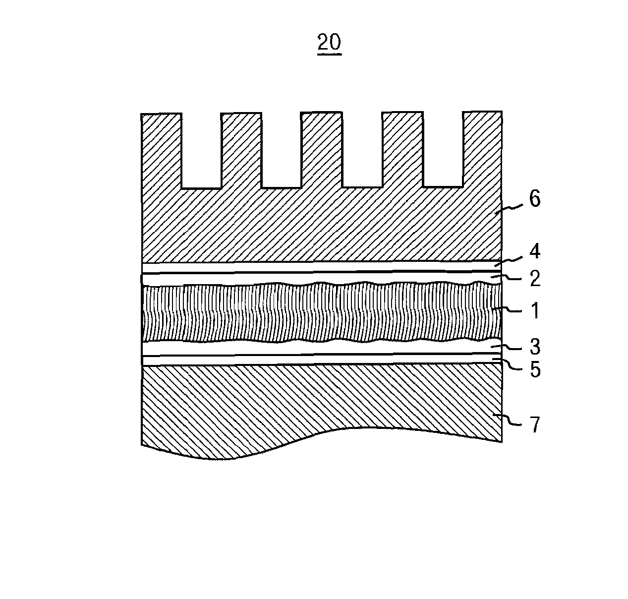
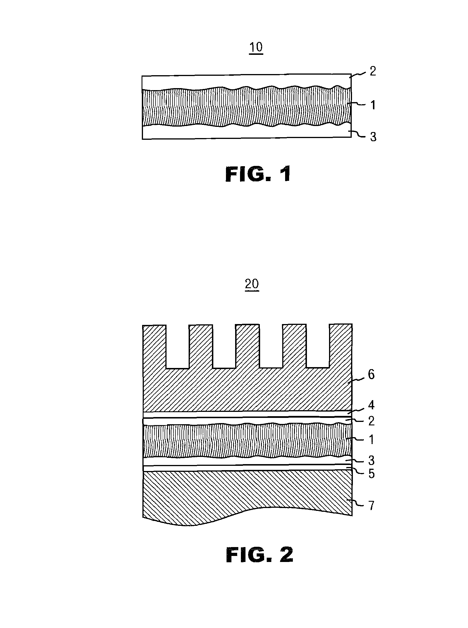
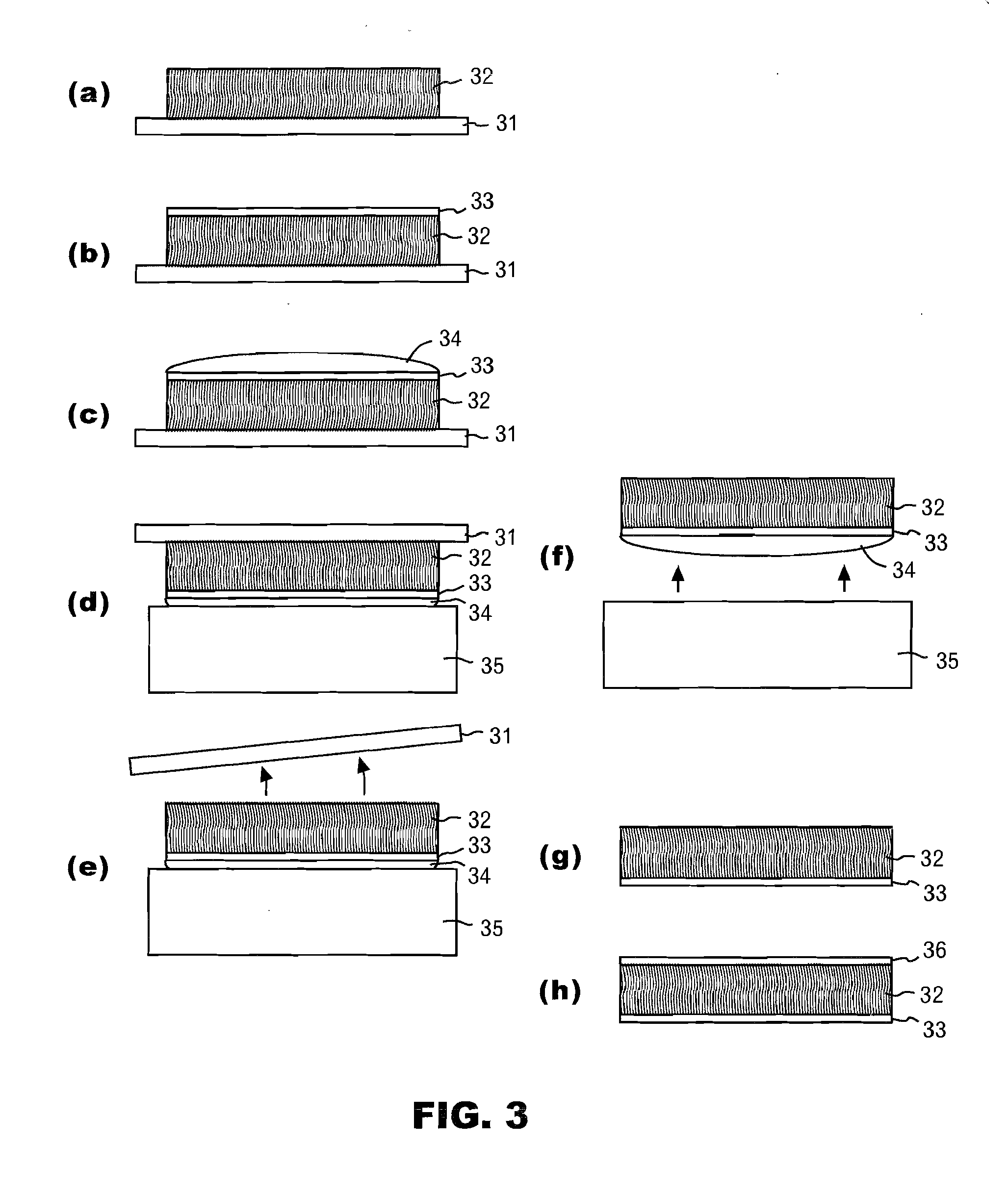
[0013] In the present invention, in order to reduce contact resistance, metal layers are provided between surfaces of a CNT layer and of a substrate or the like which faces the CNT layer. The metal layers are formed by, for example, a sputtering method as continuous metal layers on the surfaces of the layer of CNTs that are orientationally grown. Furthermore, the surfaces of the metal layers can further be thermally coupled to a substrate or the like by use of a low-melting-point metal, for example. With these components, the present invention accomplishes a thermal conduction structure with a low thermal resistance. The orientation, the high thermal conductivity and the mechanical flexibility of the CNTs are fully utilized to accomplish the above-mentioned goal. The present invention will be described in detail below with reference to the appended drawings.

[0014]FIG. 1 shows a cross section of a thermal interface structure 10 of the present invention. The thermal interface structu...


PUM

PropertyMeasurementUnit
thicknessaaaaaaaaaa
temperatureaaaaaaaaaa
thicknessaaaaaaaaaa

Abstract

A thermal interface structure includes a carbon nanotube layer, in which the carbon nanotubes are oriented parallel to the direction of thermal transmission and metal layers provided on two edge surfaces of the carbon nanotube layer, the edge surfaces being perpendicular to the direction of the thermal transmission and located substantially parallel to the orientation direction at which edges of the carbon nanotubes are oriented.

Description

FIELD OF THE INVENTION [0001] The present invention relates generally to a thermal conduction structure. Specifically, the present invention relates to a thermal interface structure capable of being used in a thermal conduction module in which integrated circuit (IC) chips or the like are embedded. BACKGROUND OF THE INVENTION [0002] In recent years, the power consumption of semiconductor ICs has continued to increase with the development of higher-density ICs. The increase in the electric power leads to an increase in the amount of heat generated, and then results in one of the reasons to hinder the improvement in clock frequencies of the semiconductor ICs. For this reason, the semiconductor ICs need to be cooled at a high efficiency for further improvement in clock frequencies of the semiconductor ICs and the like. As a structure for cooling a semiconductor IC, a thermal contact material (thermal interface structure) is provided between the semiconductor IC and a heat radiating mec...

Claims


Application Information

Patent Timeline
Patent Type & Authority Applications(United States)
IPC IPC(8): H05K7/20B21D53/06
CPCH01L23/373H01L23/433H05K7/20481Y10T156/11H01L2924/0002Y10T29/49359H01L2924/00B82Y30/00H01L23/36H05K7/20
Inventor SUEOKA, KUNIAKITAIRA, YOICHI
Owner IBM CORP
Why Eureka
Try Eureka