Wafer-level MEMS package and manufacturing method thereof

a technology of mems and packaging, applied in the direction of semiconductor devices, semiconductor/solid-state device details, electrical apparatus, etc., can solve problems such as cap structure trapping

Inactive Publication Date: 2008-04-03
SEIKO EPSON CORP
View PDF3 Cites 47 Cited by
  • Summary
  • Abstract
  • Description
  • Claims
  • Application Information

AI Technical Summary

Problems solved by technology

The sealing material during its deposition, cannot find a straight acc...

Method used


Image

  • Wafer-level MEMS package and manufacturing method thereof
  • Wafer-level MEMS package and manufacturing method thereof
  • Wafer-level MEMS package and manufacturing method thereof

Examples


Embodiment Construction

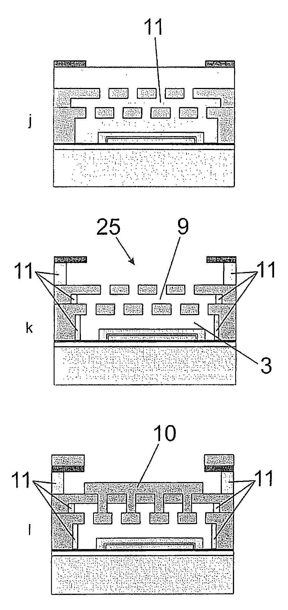
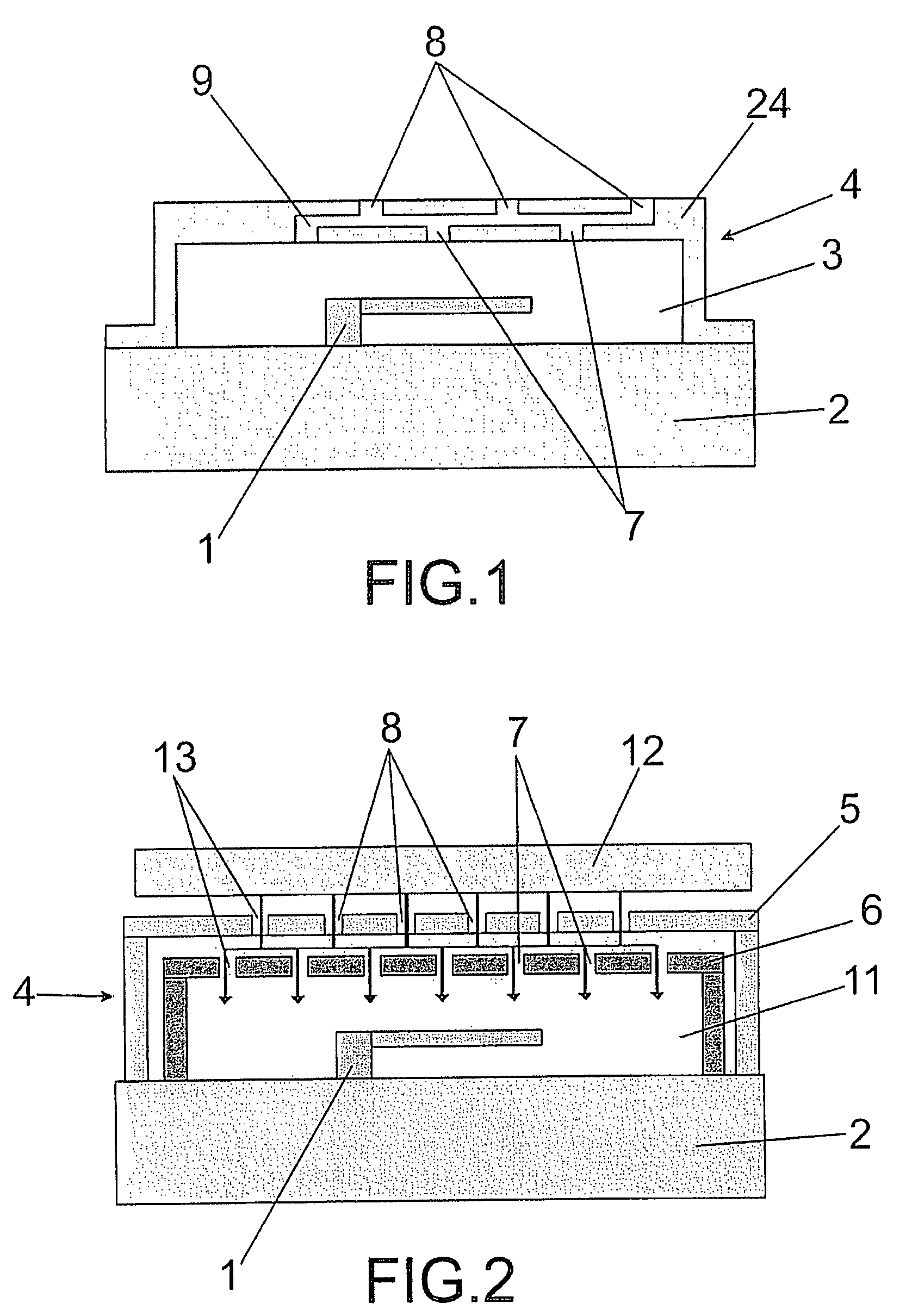
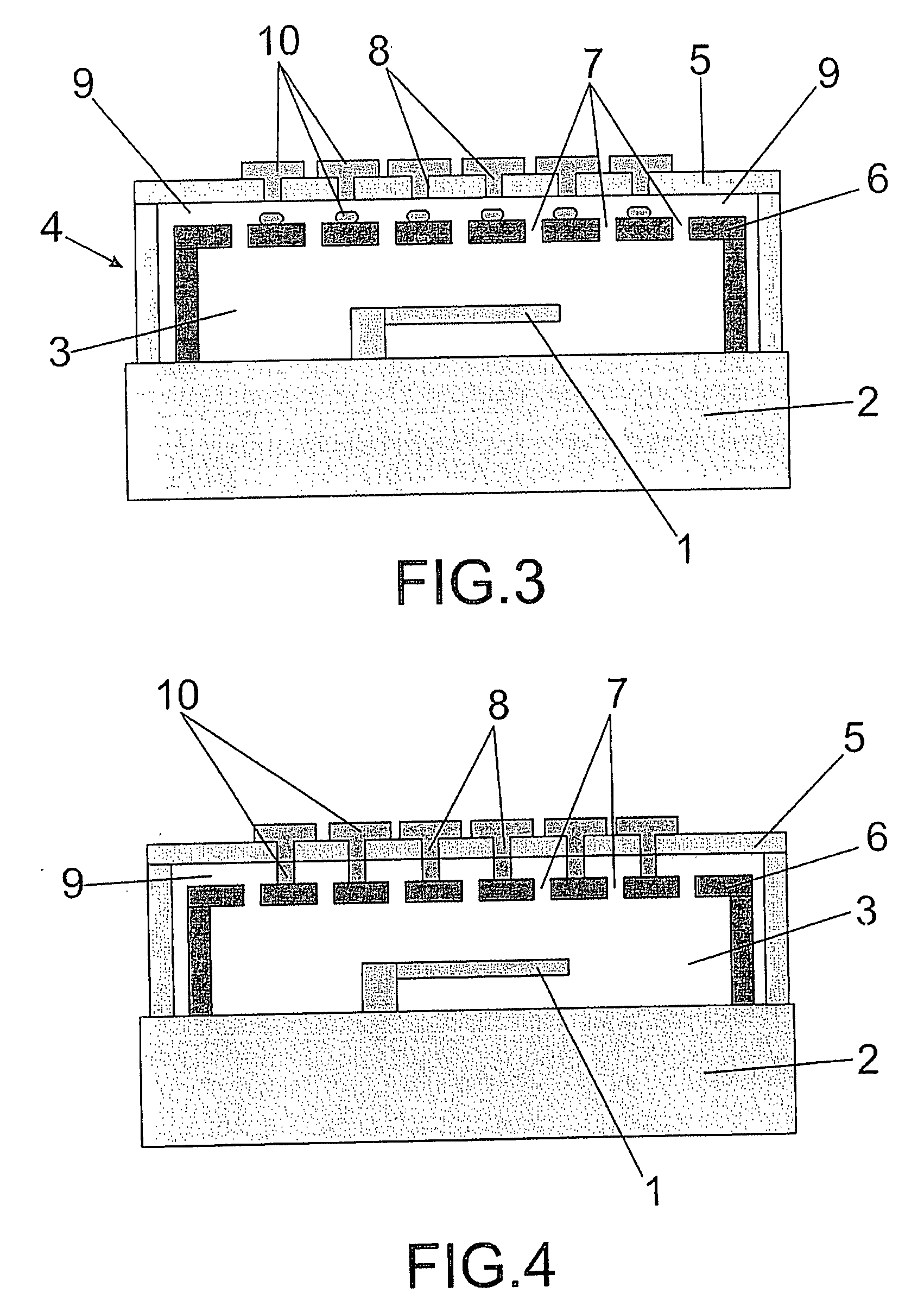
[0045]An exemplary embodiment of a MEMS package object of the invention is represented in FIG. 1, in which at least one MEMS element (1) is formed in a known manner on a base substrate (2). Preferably, the base substrate (2) is a semiconductor substrate, for example an oxidized silicon wafer, and the MEMS element (1) is formed on a planer surface of the base substrate (2).

[0046]The MEMS package comprises a cap structure (4) joined to said base substrate (2), forming a chamber (3) together with said substrate so that the MEMS element (1) is encapsulated within said chamber (3). The cap structure (4) is formed by a single protective layer (24) having a plurality of input holes (8) on its upper surface and a plurality of output holes (7) on its lower surface. The protective layer (24) includes a channel (9) which communicates said input and output holes (8,7) for the passage of an etching fluid (12) to said chamber (3). The input and output holes (8,7) are located in such a manner that...


PUM


Abstract

The present invention is related in general to a wafer-level packaging technique for micro-electro-mechanical systems (MEMS). A cap structure is provided encapsulating a MEMS element formed on a base substrate. A channel communicates etching holes provided on said cap structure, for the passage of an etching fluid to a chamber in which the MEMS element is housed. The holes are arranged in such a manner that they do not overlap, which allows the provision of a large number of etching holes above the MEMS element, but prevents a sealing material from reaching the MEMS element. The invention provides a low cost wafer-level packaging technique for MEMS devices, that reduces the total etching time of the sacrificial material and provides a reinforced protective cap structure for the MEMS package.

Description

OBJECT OF THE INVENTION[0001]The present invention is related in general to a wafer-level packaging technique for micro electromechanical systems (MEMS). More in particular the invention refers to a MEMS package and a method of manufacturing said MEMS package.[0002]It is an object of the present invention to provide a low cost wafer-level packaging technique for MEMS devices, that reduces the total etching time of the sacrificial material, and provides a reinforced protective cap structure for the MEMS devices.[0003]The present invention pertains generally to the technical field of fabrication of semiconductor devices.BACKGROUND TO THE INVENTION[0004]Micro electromechanical systems (MEMS) are widely used in many applications, such as accelerometers, optical communications, biomedical systems etc. However, MEMS are not compatible with standard integrated circuit (IC) packaging technologies, because they include generally moving components or require specific atmospheric conditions su...

Claims


Application Information

Patent Timeline
IPC IPC(8): H01L23/12H01L21/52B81C99/00
CPCB81C2203/0145B81C1/00333
Inventor CARMONA, MANUELKIHARA, RYUJIESTEVE, JAUME
Owner SEIKO EPSON CORP
Why Eureka
Try Eureka