Antenna device and wireless communication apparatus

a wireless communication and antenna device technology, applied in the direction of elongated active element feed, resonant antenna, radiating element structure, etc., can solve the problems of reducing reducing the antenna characteristics, and not being able to reduce the size of the entire devi

Inactive Publication Date: 2008-04-03
MURATA MFG CO LTD
View PDF5 Cites 31 Cited by
  • Summary
  • Abstract
  • Description
  • Claims
  • Application Information

AI Technical Summary

Benefits of technology

[0017] In order to overcome the problems described above, preferred embodiments of the present invention provide a compact and thin antenna device that can be mounted in a small area of a substrate and has a multiband capability adaptable to various applications, and provide a wireless communication apparatus.

Problems solved by technology

However, mounting an antenna device in a small area requires a reduction in the size and thickness of the antenna device, and thus may degrade the antenna characteristics.
However, known antenna devices described above have the following problems.
Although the thickness of the device can be reduced in this case, it is not possible to reduce the size of the entire device.
Moreover, since alignment including the balancing of feeding parts in the antenna device is very complicated, design work for the alignment takes a long time.
This involves difficult alignment of both configurations and antenna characteristics.
Therefore, if a multiple-resonance antenna device or a frequency-variable antenna device is produced with any one of the techniques described above, dead space that is double or more than double the normal amount is created or the size of the antenna device increases.
In other words, it is virtually impossible to incorporate such an antenna device into a wireless communication apparatus, where compactness and high board density are required.
Similar problems arise in the antenna devices disclosed in Japanese Unexamined Patent Application Publication No. 08-023218 and Japanese Unexamined Patent Application Publication No. 2004-165770.

Method used


Image

  • Antenna device and wireless communication apparatus
  • Antenna device and wireless communication apparatus
  • Antenna device and wireless communication apparatus

Examples


first preferred embodiment

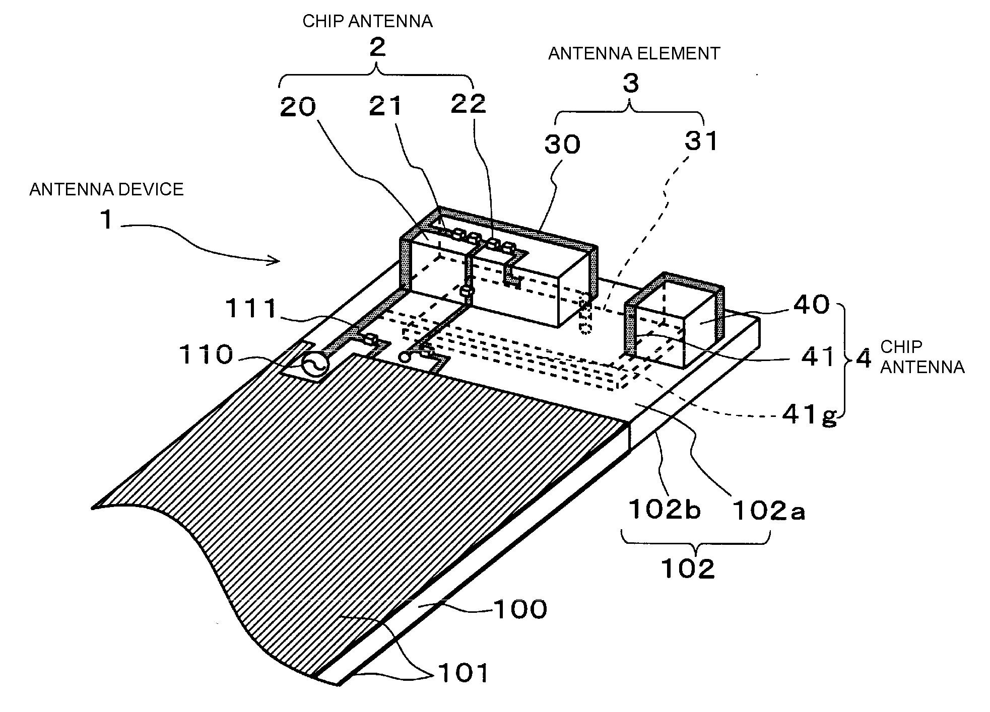
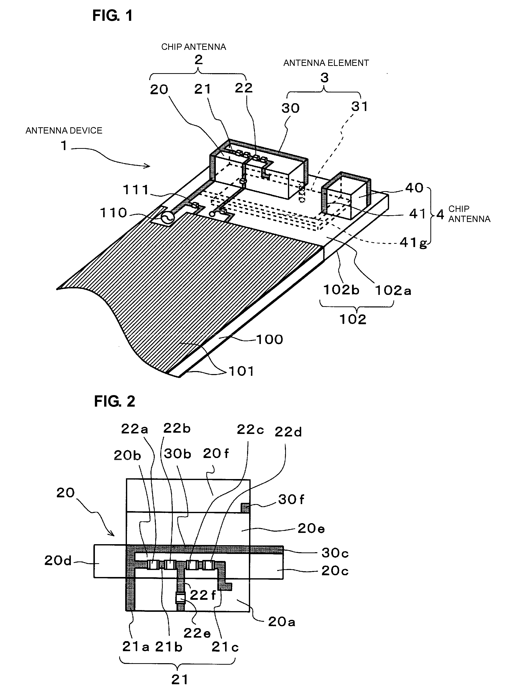
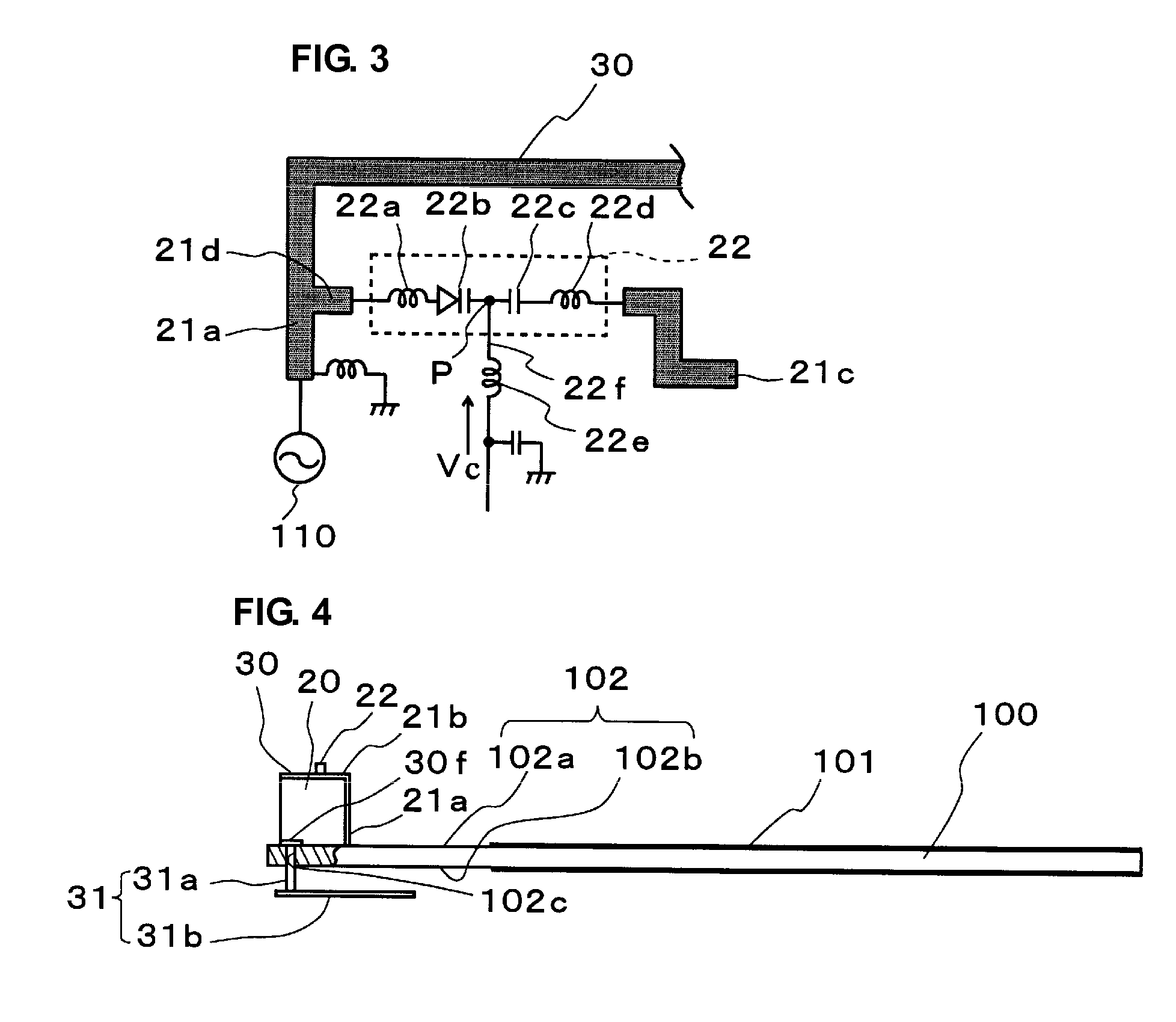
[0067]FIG. 1 is a perspective view illustrating the upper side of an antenna device according to a first preferred embodiment of the present invention. FIG. 2 is a plan view of a first chip antenna developed along sides thereof. FIG. 3 is an equivalent circuit diagram of a frequency variable circuit.

[0068] An antenna device 1 of the present preferred embodiment is mounted on a wireless communication apparatus, such as a mobile phone.

[0069] As illustrated in FIG. 1, the antenna device 1 includes a chip antenna 2 serving as a first chip antenna, an antenna element 3, and a chip antenna 4 serving as a second chip antenna.

[0070] The chip antenna 2 is a surface-mount chip antenna produced by forming a radiation electrode 21 serving as a first radiation electrode, and a frequency variable circuit 22 on the surface of a dielectric base 20.

[0071] Aground region 101 and a non-ground region 102 are disposed on both surfaces of a substrate 100, while the dielectric base 20 of the chip ante...

second preferred embodiment

[0098]FIG. 13 is a perspective view illustrating the upper side of an antenna device according to a second preferred embodiment of the present invention. FIG. 14 is a plan view illustrating the underside of the antenna device. FIG. 15 is a cutaway side view of the antenna device.

[0099] As illustrated in FIG. 13 to FIG. 15, in the antenna device of the present preferred embodiment, an auxiliary element 31 of an antenna element 3 includes a metal support 31a and a strip-shaped metal sheet 31b.

[0100] Specifically, the entire strip-shaped metal sheet 31b preferably has a substantially U-shaped configuration, and one end of the metal sheet 31b is connected to one end of the metal support 31a such that the entire metal sheet 31b is disposed over an underside 102b of a non-ground region 102.

[0101] With this configuration, the antenna element 3 can contribute to improved characteristics of the antenna device 1 and can establish another resonance.

[0102] The other configurations, function...

third preferred embodiment

[0103]FIG. 16 is a perspective view illustrating the upper side of an antenna device according to a third preferred embodiment of the present invention. FIG. 17 illustrates the underside of the antenna device. FIG. 18 is a cutaway side view of the antenna device.

[0104] As illustrated in FIG. 16, in the antenna device of the present preferred embodiment, an auxiliary element 31 of an antenna element 3 is a planar electrode.

[0105] In other words, as illustrated in FIG. 17 and FIG. 18, the auxiliary element 31 including an extraction pattern 31a and a strip-like hook-shaped conductive pattern 31b having ends extending in opposite directions is disposed on an underside 102b of a non-ground region 102. Specifically, the extraction pattern 31a of the auxiliary element 31 is connected to a connecting electrode 30f of an additional radiation electrode 30 through a through hole 102c.

[0106] This configuration contributes to the improved characteristics and reduced thickness of the antenna ...


PUM


Abstract

A compact and thin antenna device can be mounted in a small area of a substrate and has a multiband capability adaptable to various applications. The antenna device includes a chip antenna, an antenna element, and a chip antenna. The chip antenna is produced by forming a radiation electrode on the surface of a dielectric base, and mounting a frequency variable circuit on the radiation electrode. Thus, it becomes possible to obtain a resonant frequency f1 of the chip antenna and further to vary the resonant frequency f1. The antenna element is produced by adding an auxiliary element to an additional radiation electrode for the chip antenna. The chip antenna includes a radiation electrode on a dielectric base and a conductive pattern. Thus, a resonant frequency f2 and a resonant frequency f3 of the antenna element and the chip antenna, respectively, can be obtained.

Description

BACKGROUND OF THE INVENTION [0001] 1. Field of the Invention [0002] The present invention relates to an antenna device for use in mobile phones or the like, and also to a wireless communication apparatus. [0003] 2. Description of the Related Art [0004] In recent years, as the size of a wireless communication apparatus, such as a mobile phone, has decreased and density therein has increased, it is becoming necessary that an antenna device be mounted in a small area of a substrate. [0005] However, mounting an antenna device in a small area requires a reduction in the size and thickness of the antenna device, and thus may degrade the antenna characteristics. [0006] Therefore, for example, as disclosed in Japanese Unexamined Patent Application Publication No. 2000-114992, Japanese Unexamined Patent Application Publication No. 2004-023210, Japanese Unexamined Utility Model Registration Application Publication No. 07-020708, and Japanese Unexamined Patent Application Publication No. 2004-...

Claims


Application Information

Patent Timeline
Patent Type & Authority Applications(United States)
IPC IPC(8): H01Q1/24H01Q5/10
CPCH01Q1/243H01Q5/371H01Q9/42H01Q1/38
Inventor ISHIZUKA, KENICHIKAWAHATA, KAZUNARI
Owner MURATA MFG CO LTD
Why Eureka
Try Eureka