Wafer exposure device and method

a technology of exposure device and wafer, which is applied in the direction of optics, instruments, photomechanical equipment, etc., can solve the problems of deformation of microelectronic structures on some of the integrated circuits fabricated on the wafer, wafer exposure device may be subjected to deterioration of the alignment of the plural height level sensor, and sensor block misalignmen

Inactive Publication Date: 2008-04-03
QIMONDA
View PDF2 Cites 54 Cited by
  • Summary
  • Abstract
  • Description
  • Claims
  • Application Information

AI Technical Summary

Problems solved by technology

Otherwise, portions of the wafer surface would be arranged out of the focus depth, thereby resulting in defective microelectronic structures on some of the integrated circuits fabricated on the wafer.
However, when in use, the wafer exposure device may be subjected to deterioration of the alignment of the plural height level sensors.
For instance, accelerated mechanical movements due to the stepping and / or scanning steps may gradually cause misalignments of the sensor block relative to a housing of the optical exposure system or misalignments of the individual height level sensors relative to one another.
There are further influences (other than mechanical stress) which may cause effective misalignments of the height level sensors.
However, these and other influences normally are not actively observed by the tool manufacturer or by the user.

Method used


Image

  • Wafer exposure device and method
  • Wafer exposure device and method
  • Wafer exposure device and method

Examples


Embodiment Construction

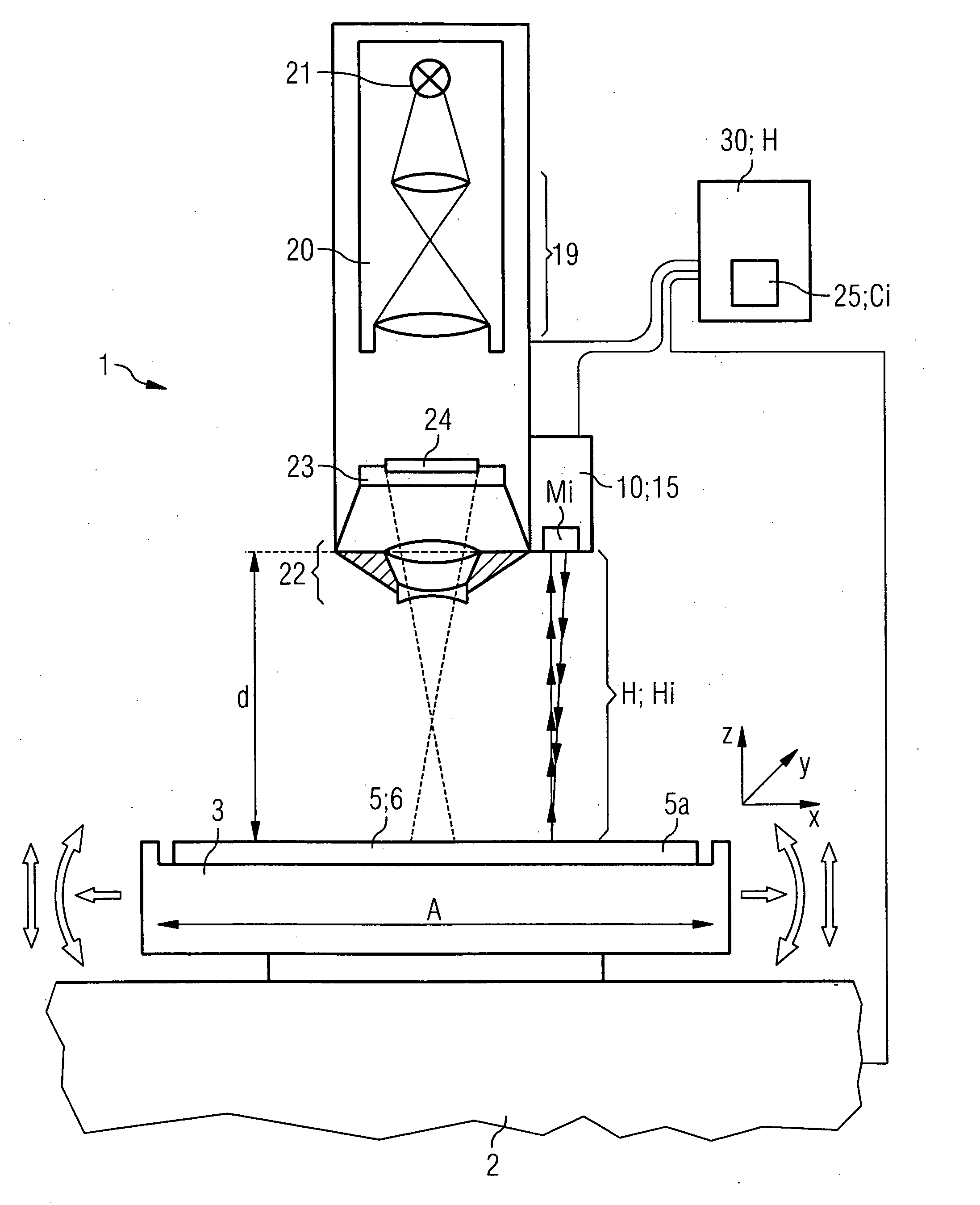
[0026]FIG. 1 illustrates a schematical view of a wafer exposure device 1. The wafer exposure device 1 preferably is a lithographic exposure device at least comprising a height level sensor device 10 and a wafer stage 2. The wafer exposure device may further include an optical exposure system 20 and a reticle stage 23 for receiving a reticle 24 to be projected on a portion of a wafer surface 5a of a wafer 5. The wafer stage 2 may comprise a wafer chuck 3 for receiving a wafer 5 thereon. The wafer chuck 3 may attract the bottom surface of the wafer by means of vacuum or very low pressure atmosphere in order to ensure safe contact of the wafer bottom surface with the contact main surface of the wafer chuck 3. The wafer stage 2 is capable of moving the wafer chuck 3 along a first lateral direction x, along a second lateral direction y and along a vertical direction z. Furthermore, the wafer stage is capable of varying and adjusting the orientation of the wafer chuck 3 as further indicat...


PUM


Abstract

A wafer exposure device includes a wafer stage. An optical exposure system exposes a wafer on the wafer stage. A sensor block measures a distance to a wafer provided on the wafer stage. The sensor block includes a plurality of height level sensors. Each height level sensor measures and outputs height level values. The wafer exposure device compares with one another the measured height level values outputted by respective height level sensors. The wafer exposure device calculates individual sensor position offset values to be attributed to the individual height level sensors. The wafer exposure device corrects the measured height level values output by the respective height level sensors using the calculated sensor position offset values of the respective height level sensor.

Description

TECHNICAL FIELD[0001]The invention is directed to the field of semiconductor manufacture and more particularly to a wafer exposure devices and to methods for measuring a distance to a wafer arranged in a wafer exposure device. The invention in particular is directed to the field of wafer leveling in a lithographic exposure device.BACKGROUND[0002]In the field of semiconductor manufacture, integrated circuits are produced on wafers or semiconductor substrates, like silicon substrates. The wafers are subjected to a plurality of processing steps, some of the processing steps comprising lithographic exposure of the wafer using a lithographic exposure device. Typically, a reticle is projected onto the wafer, thereby transferring mask patterns of the reticle onto the wafer (that is, onto a layer provided on the wafer and to be patterned lithographically. In most cases, a radiation-sensitive layer like a resist layer is provided on the substrate or on another layer (arranged on above substr...

Claims


Application Information

Patent Timeline
Patent Type & Authority Applications(United States)
IPC IPC(8): G03B27/52
CPCG03F7/7085H01L21/681G03F9/7088G03F9/7026
Inventor HOMMEN, HEIKOBIRNSTEIN, NORMANSCHUMACHER, KARLSTAECKER, JENS
Owner QIMONDA
Why Eureka
Try Eureka