Method of fabricating semiconductor device

a semiconductor and device technology, applied in the field of semiconductor device manufacturing, can solve the problems of high cost of high-performance exposure equipment development and photoresist pattern deformation during formation, and achieve the effect of reducing line width

Inactive Publication Date: 2008-04-10
SAMSUNG ELECTRONICS CO LTD
View PDF8 Cites 6 Cited by
  • Summary
  • Abstract
  • Description
  • Claims
  • Application Information

AI Technical Summary

Benefits of technology

[0008]It is therefore a feature of an embodiment of the present invention to provide a method of fabricating a semiconductor device with fine patterns having reduced linewidth.

Problems solved by technology

However, when the linewidth of the semiconductor device is small, the photoresist pattern may deform during formation thereof.
However, development of high-performance exposure equipment may be cost-consuming and may require a stable light source and exposure technology.

Method used


Image

  • Method of fabricating semiconductor device
  • Method of fabricating semiconductor device
  • Method of fabricating semiconductor device

Examples


Embodiment Construction

[0025]Korean Patent Application No. 2006-98060, filed on Oct. 9, 2006, in the Korean Intellectual Property Office, and entitled: “Method of Fabricating Semiconductor Device,” is incorporated by reference herein in its entirety.

[0026]The present invention will now be described more fully hereinafter with reference to the accompanying drawings, in which exemplary embodiments of the invention are illustrated. The invention may, however, be embodied in different forms and should not be construed as limited to the embodiments set forth herein. Rather, these embodiments are provided so that this disclosure will be thorough and complete, and will fully convey the scope of the invention to those skilled in the art.

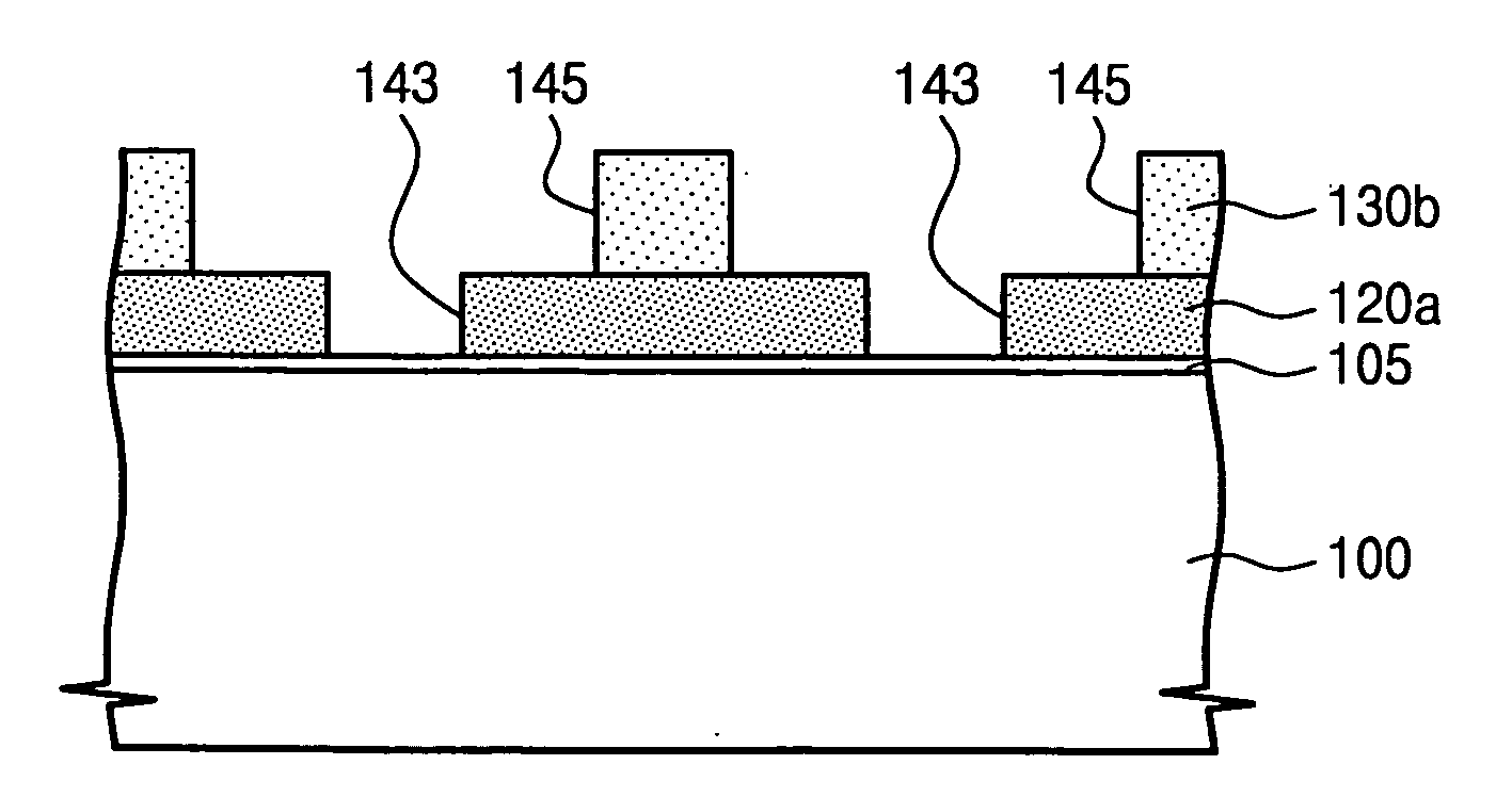
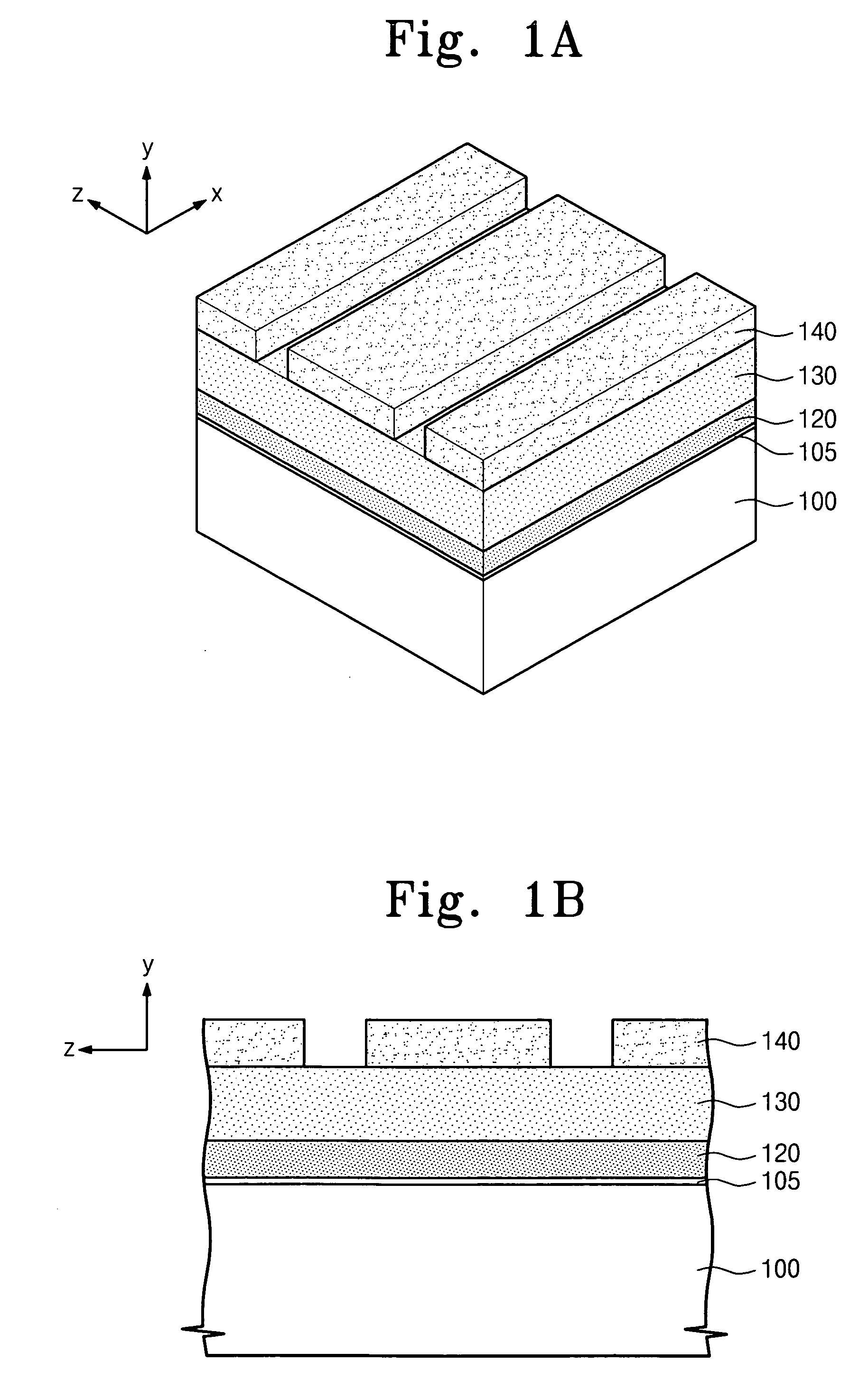
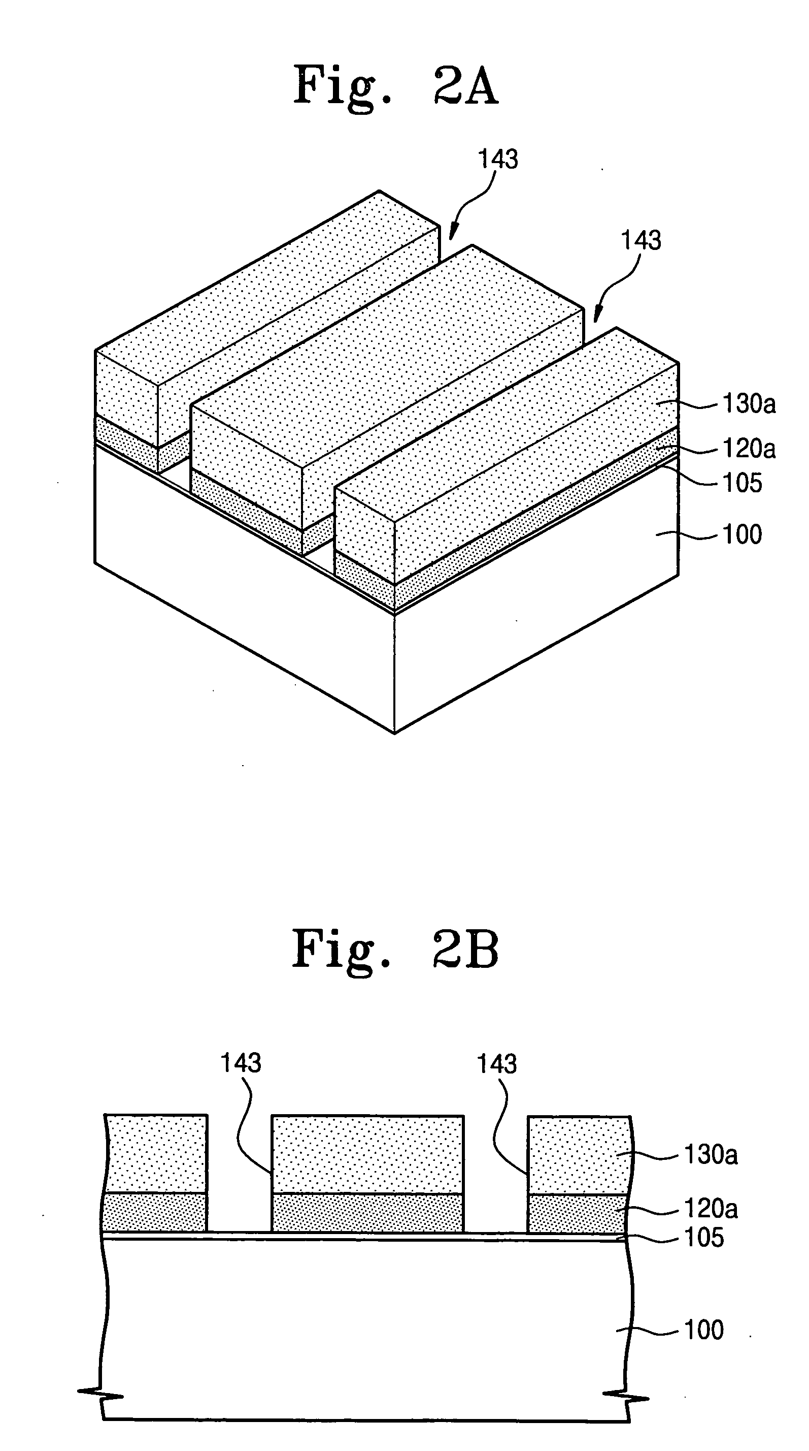
[0027]In the figures, the dimensions of layers and regions may be exaggerated for clarity of illustration. It will also be understood that when a layer or element is referred to as being “on” another layer or substrate, it can be directly on the other layer or substrate, or interv...


PUM

PropertyMeasurementUnit
widthaaaaaaaaaa
semiconductoraaaaaaaaaa
circular shapesaaaaaaaaaa

Abstract

A method of fabricating a semiconductor device includes forming a first mask layer on a semiconductor substrate, forming a second mask layer on the first mask layer, patterning the first mask layer and the second mask layer to form a first mask pattern and a second mask pattern, respectively, the first and second mask layers having a plurality of first openings, widening an upper portion of the plurality of first openings to form a second fine mask pattern with a plurality of second openings having a larger width as compared to a width of the plurality of the first openings, forming a third mask pattern in the plurality of first and second openings, removing the second fine mask pattern, and etching the first mask pattern to form a first fine mask pattern.

Description

BACKGROUND OF THE INVENTION[0001]1. Field of the Invention[0002]The present invention disclosed herein relates to a method of fabricating a semiconductor device. More particularly, there present invention relates to a method of fabricating a semiconductor device with reduced linewidths.[0003]2. Description of the Related Art[0004]In general, as the integration level of a semiconductor device increases, the linewidth required to realize the device may be decreased. Accordingly, the width of a photoresist pattern, used as a mask, may be reduced in order to decrease the linewidth of the semiconductor device. However, when the linewidth of the semiconductor device is small, the photoresist pattern may deform during formation thereof.[0005]In addition, high-performance exposure equipment may be required to obtain an appropriately small linewidth of the semiconductor device. However, development of high-performance exposure equipment may be cost-consuming and may require a stable light so...

Claims


Application Information

Patent Timeline
Patent Type & Authority Applications(United States)
IPC IPC(8): G03F7/26
CPCH01L21/0337H01L21/0338H01L21/3081H01L21/3086H01L28/60H01L21/31144H01L21/32139H01L21/76816H01L21/3088
Inventor YOUN, HYOUNG-JOO
Owner SAMSUNG ELECTRONICS CO LTD
Why Eureka
Try Eureka