Semiconductor laser

Inactive Publication Date: 2008-04-17
OSRAM OPTO SEMICON GMBH & CO OHG
View PDF20 Cites 37 Cited by
  • Summary
  • Abstract
  • Description
  • Claims
  • Application Information

AI Technical Summary

Benefits of technology

[0006] It is an object of the present invention to provide a semiconductor laser which sup

Problems solved by technology

The small thickness of the SiO2 film can have a disadvantageous effect on the electrical pro

Method used


Image

  • Semiconductor laser
  • Semiconductor laser
  • Semiconductor laser

Examples


Example

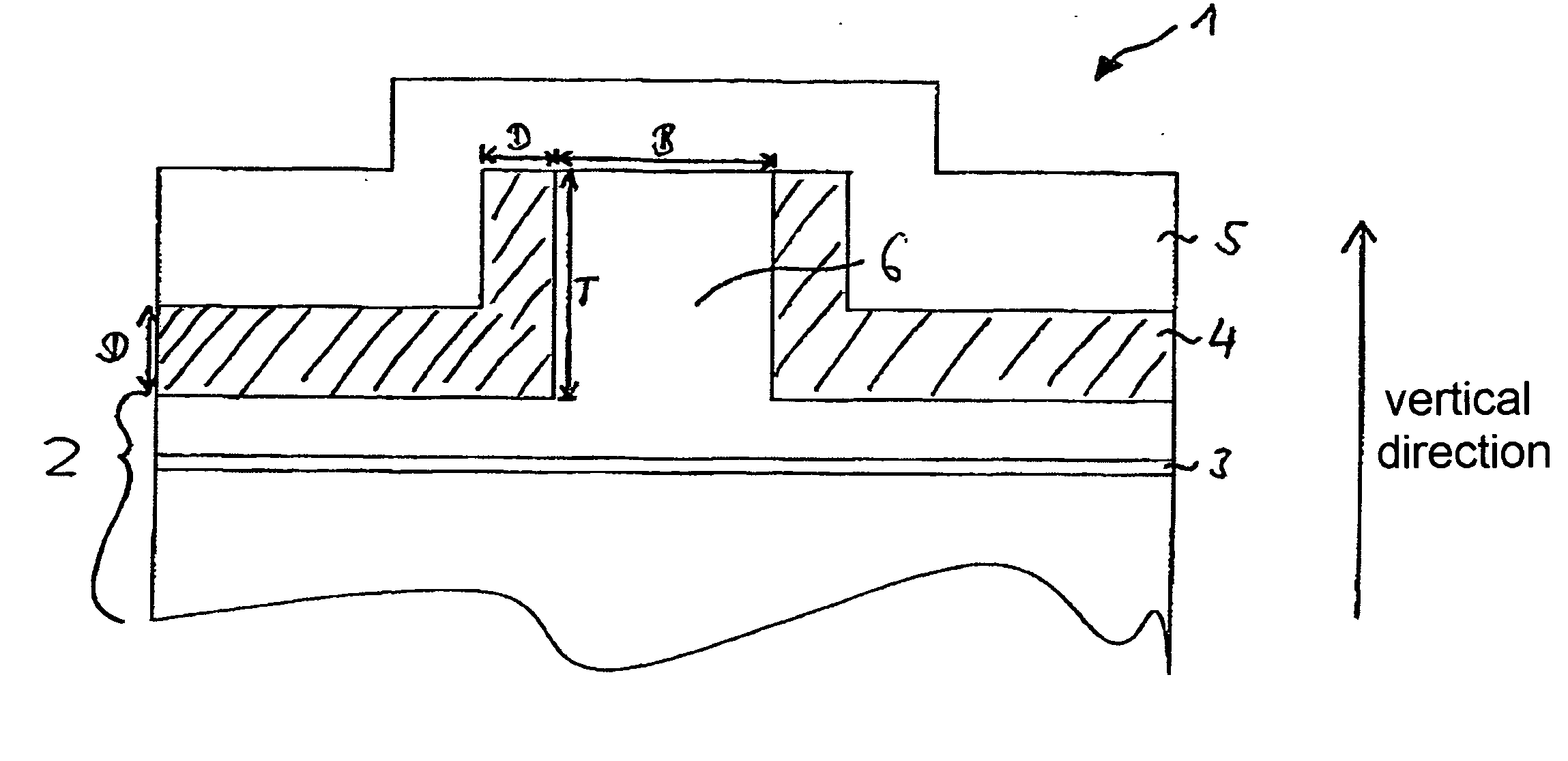
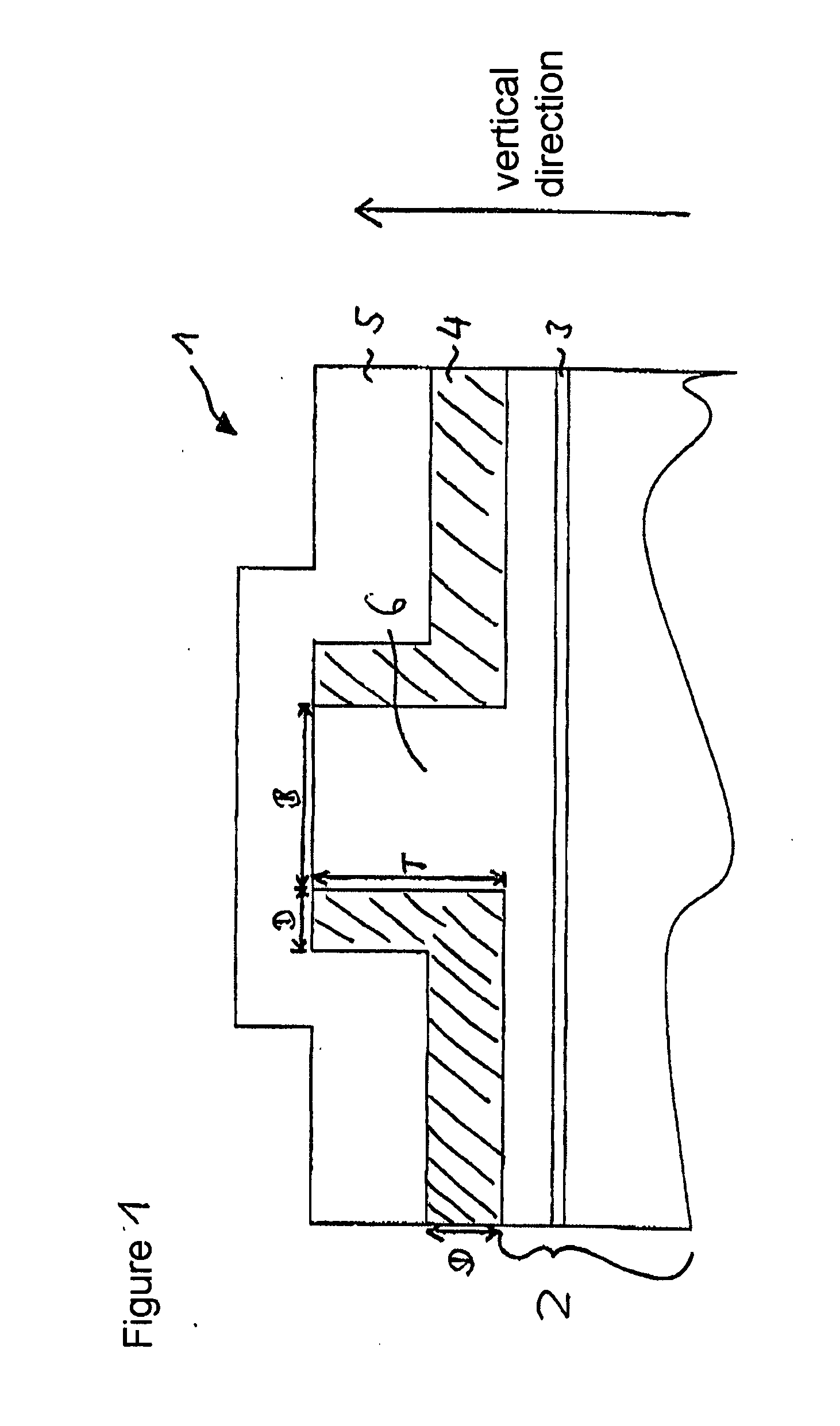
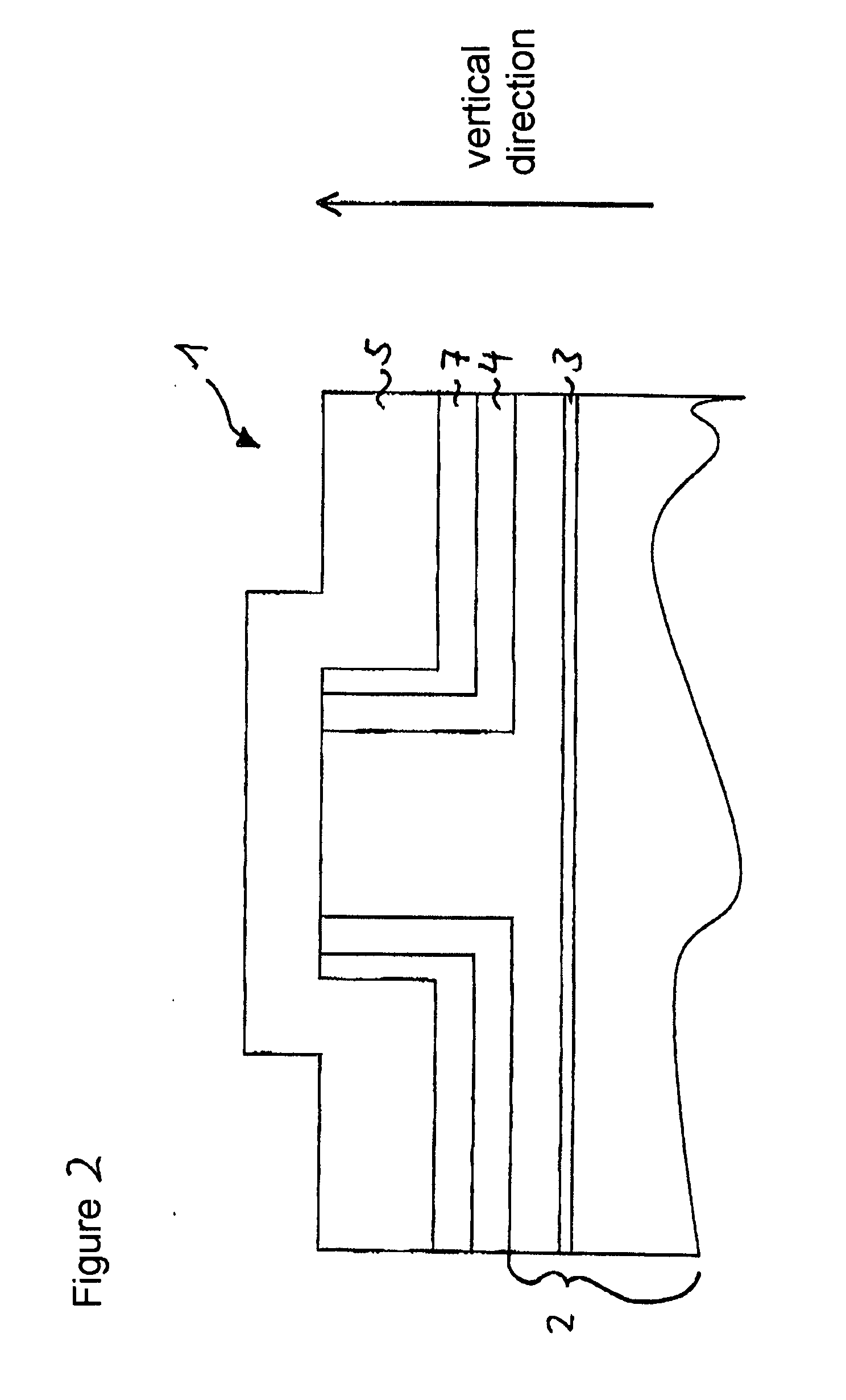
DETAILED DESCRIPTION OF THE DRAWINGS

[0056] In FIGS. 11a and 11b, the threshold gain Gth is plotted against the etching depth in a respective graph for two conventional ridge lasers.

[0057]FIG. 11a relates to a ridge laser having a ridge width of 1.5 μm, while FIG. 11b relates to a ridge laser having a ridge width of 5 μm. The various curves specify the threshold gain profile for various modes (curve I: fundamental mode; curve II: 1st order; curve III: 2nd order; curve IV: 3rd order; curve V: 4th order; curve VI: 6th order; curve VII: 9th order).

[0058] Both graphs reveal that the threshold gain decreases as the etching depth increases. Likewise, the threshold gain decreases as the ridge width increases. What is problematic in both cases is that higher-order modes occur at increasing etching depth. As emerges from FIG. 11b, in the case of a wider ridge the higher-order modes already arise at smaller etching depths.

[0059] Possible options as to how higher modes can be attenuated des...


PUM


Abstract

A semiconductor laser comprising a semiconductor layer sequence (2) comprising an active zone (3) for generating electromagnetic radiation, and an absorber zone for attenuating higher modes. The absorber zone is arranged within the semiconductor layer sequence (2) or adjoins the semiconductor layer sequence (2).

Description

RELATED APPLICATION [0001] This patent application claims the priority of German patent application 10 2006 046 297.1 filed Sep. 29, 2006, the disclosure content of which is hereby incorporated by reference. FIELD OF THE INVENTION [0002] The invention relates to a semiconductor laser, in particular to a single-mode semiconductor laser. BACKGROUND OF THE INVENTION [0003] Lasers having good beam quality, high coherence length and small spectral width are desirable or even necessary for many applications. These properties can be obtained in particular with single-mode lasers such as, for example, DFB lasers, surface emitting semiconductor lasers (VCSEL—Vertical Cavity Surface Emitting Laser) or ridge lasers. [0004] The patent specification U.S. Pat. No. 6,711,197 B2 describes a ridge laser having a p-type cladding layer composed of AlGaN, wherein an SiO2 film and an Si film disposed downstream of the SiO2 film for absorption of higher modes are arranged on the p-type cladding layer. [0...

Claims


Application Information

Patent Timeline
IPC IPC(8): H01S5/22
CPCH01S5/1064H01S5/1237H01S5/2022H01S5/22H01S5/2205H01S5/2214H01S2304/12H01S5/2219H01S5/222H01S5/2231H01S5/2232H01S5/32341H01S2301/166H01S5/2216
Inventor EICHLER, CHRISTOPHLELL, ALFREDRUMBOLZ, CHRISTIAN
Owner OSRAM OPTO SEMICON GMBH & CO OHG
Why Eureka
Try Eureka