Bragg refractive waveguide edge transmitting semiconductor laser with low horizontal divergence angle

A technology of Bragg reflection and divergence angle, which is applied to the structure of optical waveguide semiconductors, etc., can solve the problems of complex far-field patterns, epitaxial growth, preparation process, demanding working current and temperature, narrow lateral far-field divergence angle, etc., to achieve Improve the effect of catastrophic damage on the end face, stable single transverse mode operation, and large gain and loss difference

Active Publication Date: 2012-01-18
CHANGCHUN INST OF OPTICS FINE MECHANICS & PHYSICS CHINESE ACAD OF SCI
View PDF4 Cites 30 Cited by
  • Summary
  • Abstract
  • Description
  • Claims
  • Application Information

AI Technical Summary

Problems solved by technology

However, due to the larger volume of the structured light mode of these lasers, the problem of multi-mode operation is more serious, which will make the far-field pattern complex and the quality of the laser beam will be greatly reduced, so the lateral far-field divergence angle (full width at half maximum FWHM) can only reach more than a dozen degrees, it is difficult to obtain a narrower lateral far-field divergence angle
In addition, these lasers are very sensitive to the small refractive index changes caused by the deviation of the composition of the epitaxial growth structure or the temperature change, and the power, efficiency, and mode of the laser are unstable, so the epitaxial growth, preparation process, and operating current and temperature are demanding.

Method used


Image

  • Bragg refractive waveguide edge transmitting semiconductor laser with low horizontal divergence angle
  • Bragg refractive waveguide edge transmitting semiconductor laser with low horizontal divergence angle
  • Bragg refractive waveguide edge transmitting semiconductor laser with low horizontal divergence angle

Examples


Embodiment 1

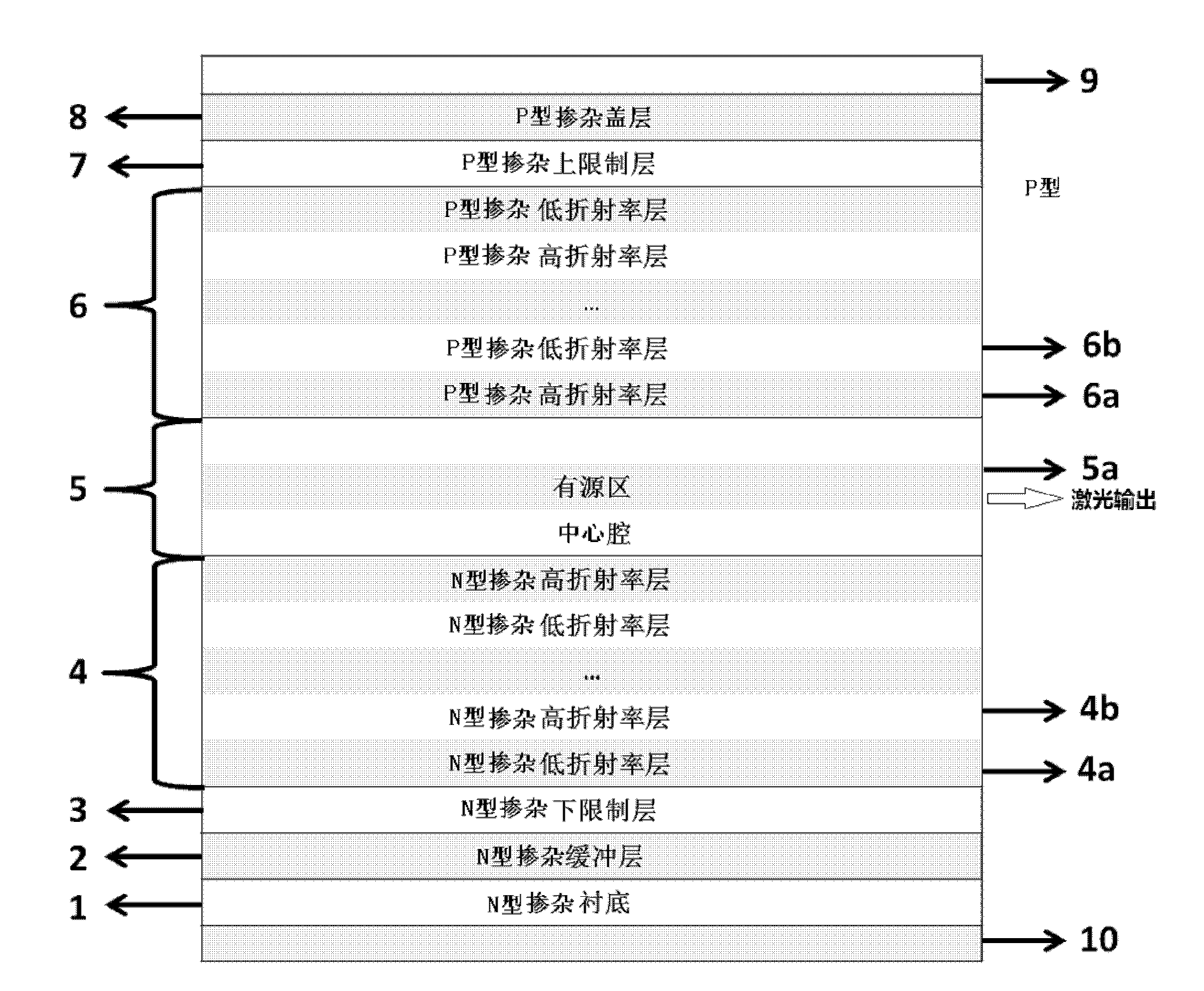
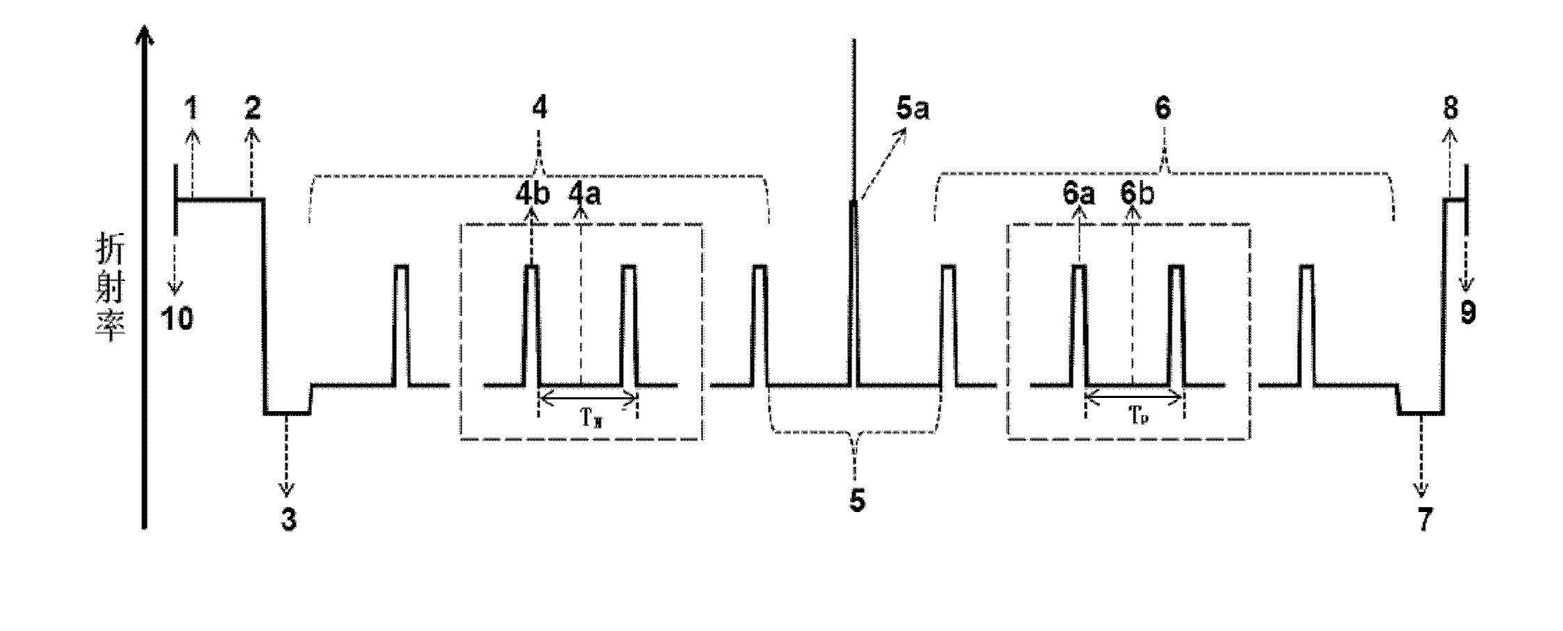
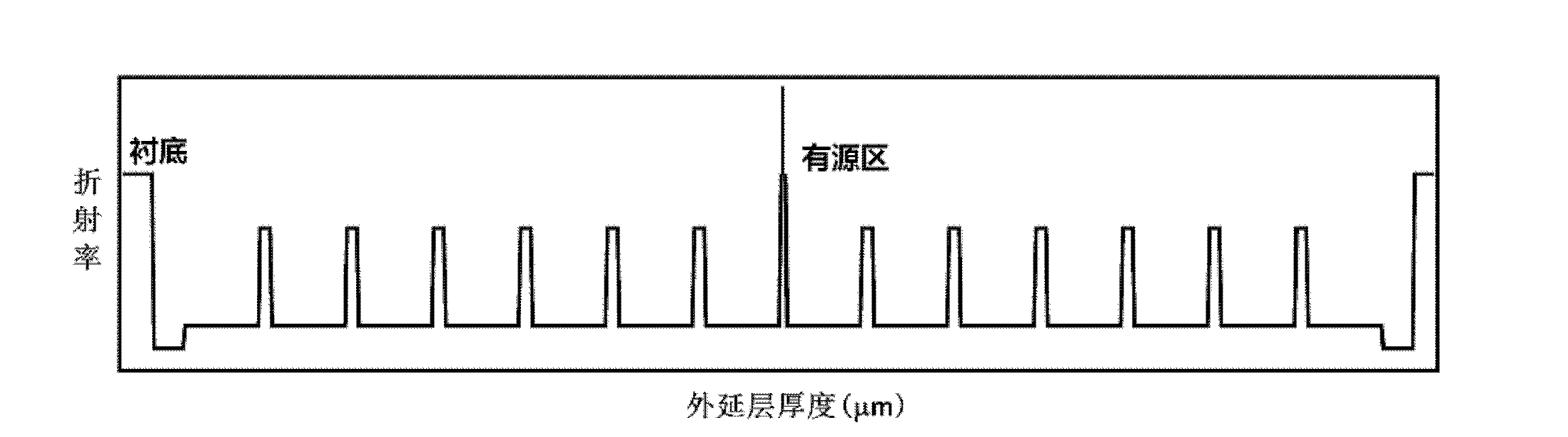
[0047] Such as Figure 3(a) , 3(b) , 3(c) is a schematic diagram of the refractive index distribution, fundamental transverse mode near-field and far-field distribution of a symmetrical low lateral divergence Bragg reflective waveguide edge-emitting semiconductor laser (wavelength 980nm). Its N-plane and P-plane waveguides both use 6 pairs of Al 0.1 Ga 0.9 As / Al 0.3 Ga 0.7 As periodic waveguide, the arrangement period T of the high and low refractive index layers of the lower waveguide layer 4 N The high and low refractive index layers of the upper waveguide layer 6 are arranged with a period T P Equal, the material and thickness of the high and low refractive index layers in each cycle of the upper waveguide layer 6 and the lower waveguide layer 4 are respectively the same. The active area is located in the center of the central cavity, using In 0.2 Ga 0.8 As / GaAs double quantum wells (QWs). As can be seen from the near-field distribution of the fundamental mode in F...

Embodiment 2

[0049] Such as Figure 4(a) , 4(b) , 4(c) is a schematic diagram of the refractive index distribution, the near-field and far-field distribution of the fundamental transverse mode of an asymmetric low lateral divergence Bragg reflective waveguide edge-emitting semiconductor laser (wavelength is 980nm), and its N surface and P-plane waveguides respectively use 8 pairs and 4 pairs of Al 0.1 Ga 0.9 As / Al 0.3 Ga 0.7 As periodic waveguide; the material and thickness of the high and low refractive index layers in each period of the lower waveguide layer 4 and the upper waveguide layer 6 are the same, but the period logarithm of the upper waveguide layer 6 is smaller than that of the lower waveguide layer 4 . The active area uses In 0.2 Ga 0.8 As / GaAs double quantum wells (QWs). In the figure, 4(a) is the refractive index distribution, 4(b) and 4(c) are the transverse near-field distribution and far-field distribution of the fundamental transverse mode, respectively. It can b...

Embodiment 3

[0051] Such as Figure 5 As shown, it is a schematic diagram of the refractive index distribution of an asymmetric low lateral divergence Bragg reflective waveguide edge-emitting semiconductor laser, the high refractive index layer 4b in its lower waveguide layer 4 and the high refractive index layer in the upper waveguide layer 6 6a. The material and thickness of the low refractive index layer 4a in the lower waveguide layer 4 and the low refractive index layer 6b in the upper waveguide layer 6 are not exactly the same, and the period logarithms in the two waveguide layers can be the same or different . The central cavity 5 is located between the lower waveguide layer 4 and the upper waveguide layer 6, and is a defect layer common to the two photonic crystals. Its refractive index and thickness are not exactly the same as those of any layer in the period of the lower waveguide 4 and the upper waveguide 6. The defect layer is designed so that the lateral transmission constant...


PUM


Abstract

The invention relates to a Bragg refractive waveguide edge transmitting semiconductor laser with a low horizontal divergence angle, wherein the P electrode of the laser is placed on the top face of a cover layer and is electrically connected onto the cover layer; the N electrode is positioned on the back face of a substrate and is electrically connected to the substrate; a center cavity is positioned between an upper waveguide layer and a lower waveguide layer; an active area is inserted in the center cavity; a Bragg refractive waveguide formed by periodically distributing a plurality of layers of N-doped materials with a high refractive index and a low refractive index is adopted in the lower waveguide layer on; and a Bragg refractive waveguide formed by periodically distributing a plurality of layers of P-doped materials with a high refractive index and a low refractive index is adopted in the upper waveguide layer. The Bragg refractive waveguide edge transmitting semiconductor laser with the low horizontal divergence angle has the advantages that: effects such as catastrophic damage, hole burning, electric heat overburning, beam filamentization and the like on the end face of the traditional edge transmitting semiconductor laser can be effectively improved, and the laser can realize the large mode-volume and stable single-transverse-mode work because of the great gain loss difference between a basic mode and a high-order mode, the full wave at half maximum (FWHM) of the transverse far-field divergence angle of the laser can reach below 10 DEG.

Description

Technical field: [0001] The invention belongs to the technical field of semiconductor lasers, and relates to a Bragg reflective waveguide edge-emitting semiconductor laser with a low lateral laser beam divergence angle. Background technique: [0002] High-power semiconductor lasers have extremely important applications in laser material processing, pumping, medical treatment, sensing, display technology, frequency conversion, space communication and national defense. With the expansion of application fields, the performance requirements of semiconductor lasers are also increasing. High, such as high output power, stable single-mode characteristics, low far-field divergence angle, high beam quality, etc. [0003] The traditional semiconductor laser structure includes N-face electrode, substrate, buffer layer, lower confinement layer, lower waveguide layer, active region, upper waveguide layer, upper confinement layer, capping layer and P-face electrode from bottom to top; P-f...

Claims


Application Information

Patent Timeline
Patent Type & Authority Applications(China)
IPC IPC(8): H01S5/22
Inventor 汪丽杰佟存柱王立军曾玉刚刘云张俊
Owner CHANGCHUN INST OF OPTICS FINE MECHANICS & PHYSICS CHINESE ACAD OF SCI
Why Eureka
Try Eureka