Contact structure for semiconductor devices

a contact structure and semiconductor technology, applied in the direction of semiconductor/solid-state device manufacturing, transistors, electrical devices, etc., can solve the problem that metals also have low resistivity for better performan

Inactive Publication Date: 2008-04-24
AGENCY FOR SCI TECH & RES
View PDF6 Cites 5 Cited by
  • Summary
  • Abstract
  • Description
  • Claims
  • Application Information

AI Technical Summary

Benefits of technology

[0005] Embodiments of the present invention offer additional alternatives to control the barrier height in semiconductor devices. Barrier heights are successfully controlled through contact structure configured according to embodiments of the present invention.
[0006] In accordance with one aspect of the present invention, there is provided a contact structure for semiconductor devices. In one embodiment, the semiconductor device has a substrate of one type of semiconductor material, such as silicon. A contact structure is formed on the substrate, and the contact structure is formed of a compound of a metal and a second type of semiconductor material, such as germanium. The contact structure according to embodiments of the present invention therefore includes a semiconductor material, formed on a substrate which is of a different type of semiconductor material. An effect of either increased or decreased barrier height is obtained in a semiconductor device employing such a contact structure.

Problems solved by technology

However, most devices require that the metal also have low resistivity for better performance.

Method used


Image

  • Contact structure for semiconductor devices
  • Contact structure for semiconductor devices
  • Contact structure for semiconductor devices

Examples


Embodiment Construction

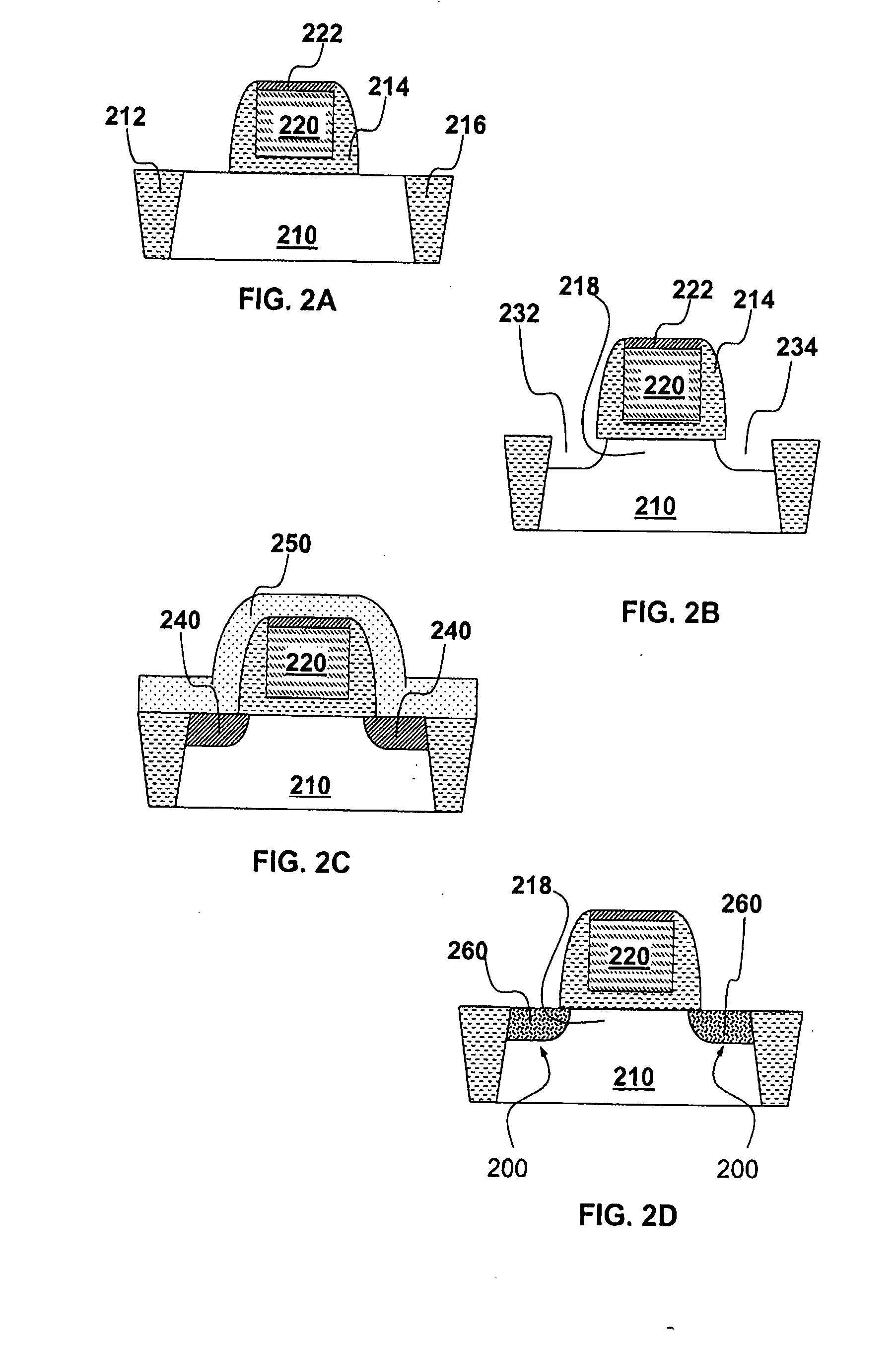
[0019] For the purpose of illustration, embodiments of the present invention will be described to structures and methods of forming the structures, which may be described as applicable in various semiconductor devices. Nevertheless, it will be understood by one skilled in the art that embodiments of the present invention are applicable to semiconductor devices which are of different types from the examples shown here.

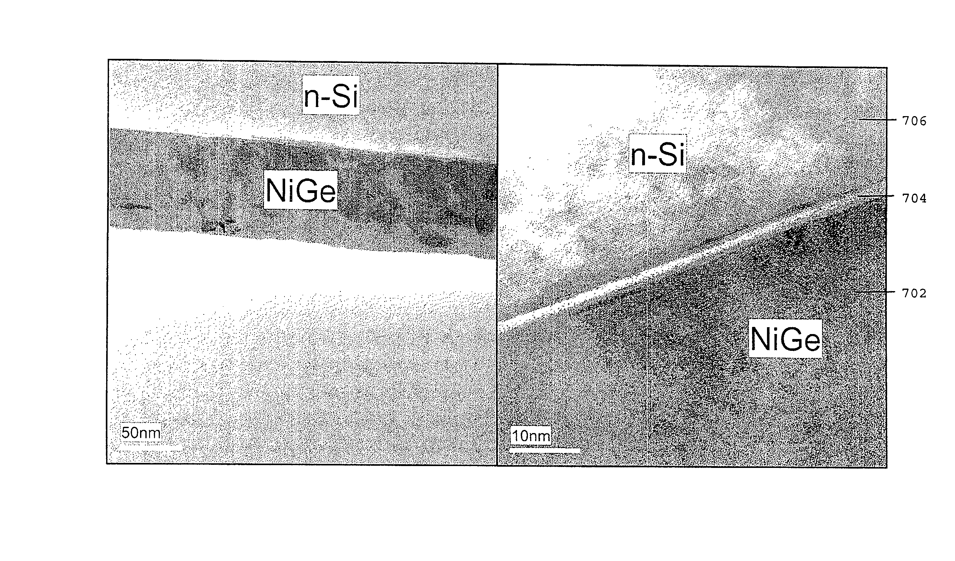
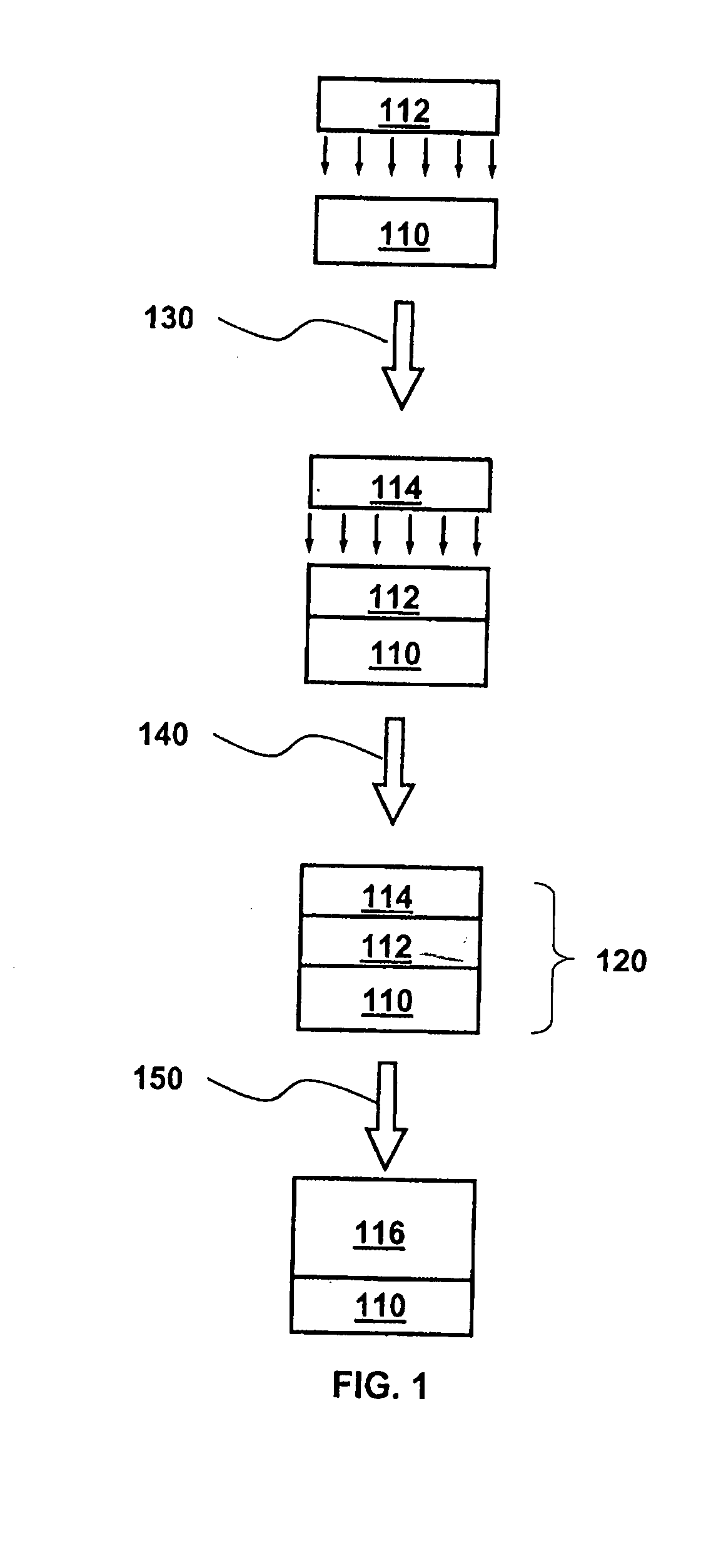
[0020] As shown in FIG. 1, a contact structure for semiconductor devices according to one embodiment of the present invention includes a substrate 110, made of a first type of semiconductor material, for example silicon. After the substrate 110 undergoes a cleaning process, a layer 112 of a second type of semiconductor material, for example germanium, is deposited on substrate 110, as shown in step 130. In the present embodiment, germanium is used here due to the similar electron affinity between germanium and silicon. Upon formation of the germanium layer 112, a metal...


PUM


Abstract

A semiconductor device has a substrate of one type of semiconductor material, such as silicon. A contact structure is formed on the substrate, and the contact structure is formed of a compound of a metal and a second type of semiconductor material, such as germanium. The contact structure according to embodiments of the present invention include a semiconductor material which a different semiconductor material forming the substrate. Higher or lower barrier height is obtained by embodiment of the invention. A method for forming a contact structure in which a substrate of one type of semiconductor material is provided. A layer of another different semiconductor material is formed on the substrate. A layer of metal is then formed on the layer of the other different semiconductor material. Upon annealing, a contact structure is formed on the substrate, which is a compound of the metal and the other different semiconductor material, onto the substrate.

Description

FIELD OF THE INVENTION [0001] The present invention relates to semiconductor devices. In particular, it relates to contact structure for semiconductor devices. BACKGROUND OF THE INVENTION [0002] In a Metal-Semiconductor interface, there exists a rectifying barrier known as Schottky barrier, the magnitude of this barrier called Schottky barrier height depends on the work-functions of the Metal-Semiconductor combination used. Unlike Semiconductors, work-functions are intrinsic properties of metals; little could be done but to choose the metal with the right work-functions for the desired effect: high barrier height as rectifiers or low barrier height to lower contact resistance. However, most devices require that the metal also have low resistivity for better performance. Faced with these restrictions, Metal-Semiconductor compounds, such as Metal-Silicides were introduced resulting in Silicide-Semiconductor interface which provided device manufacturers with additional choices. As a ma...

Claims


Application Information

Patent Timeline
Patent Type & Authority Applications(United States)
IPC IPC(8): H01L29/80H01L21/335
CPCH01L21/28044H01L21/28518H01L21/28537H01L29/456H01L29/7839H01L29/4925H01L29/66636H01L29/66643H01L29/47
Inventor CHI, DONG ZHITAN, CHENG CHEH DENNISCHUA, CHEE TEE
Owner AGENCY FOR SCI TECH & RES
Why Eureka
Try Eureka