Integrated matching network and method for manufacturing integrated matching networks

a matching network and integrated technology, applied in the field of integrated matching networks, can solve the problems of poor heat dissipation properties, difficult reproducibility, and difficulty in controlling the length of wirebonds,

Active Publication Date: 2008-05-01
NXP USA INC
View PDF5 Cites 3 Cited by
  • Summary
  • Abstract
  • Description
  • Claims
  • Application Information

AI Technical Summary

Problems solved by technology

With increasing frequencies, these inductances typically become smaller, and the control of wirebond length generally becomes more difficult.
For example, as the inductance decreases and the wirebond length decreases, reproducibility becomes more difficult.
Additionally, higher frequency base station PA devices may rely on GaAs technologies, which generally have poor heat dissipation properties.
To compensate, thinner PA dies are typically used, which generally impacts the printed inductor performance.

Method used


Image

  • Integrated matching network and method for manufacturing integrated matching networks
  • Integrated matching network and method for manufacturing integrated matching networks
  • Integrated matching network and method for manufacturing integrated matching networks

Examples


Embodiment Construction

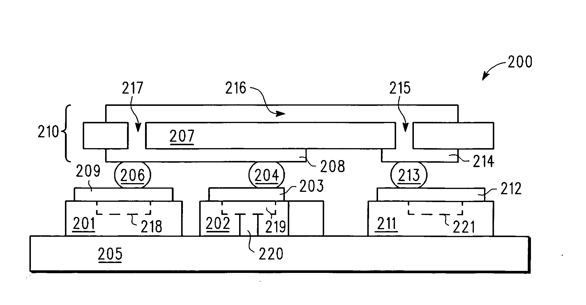
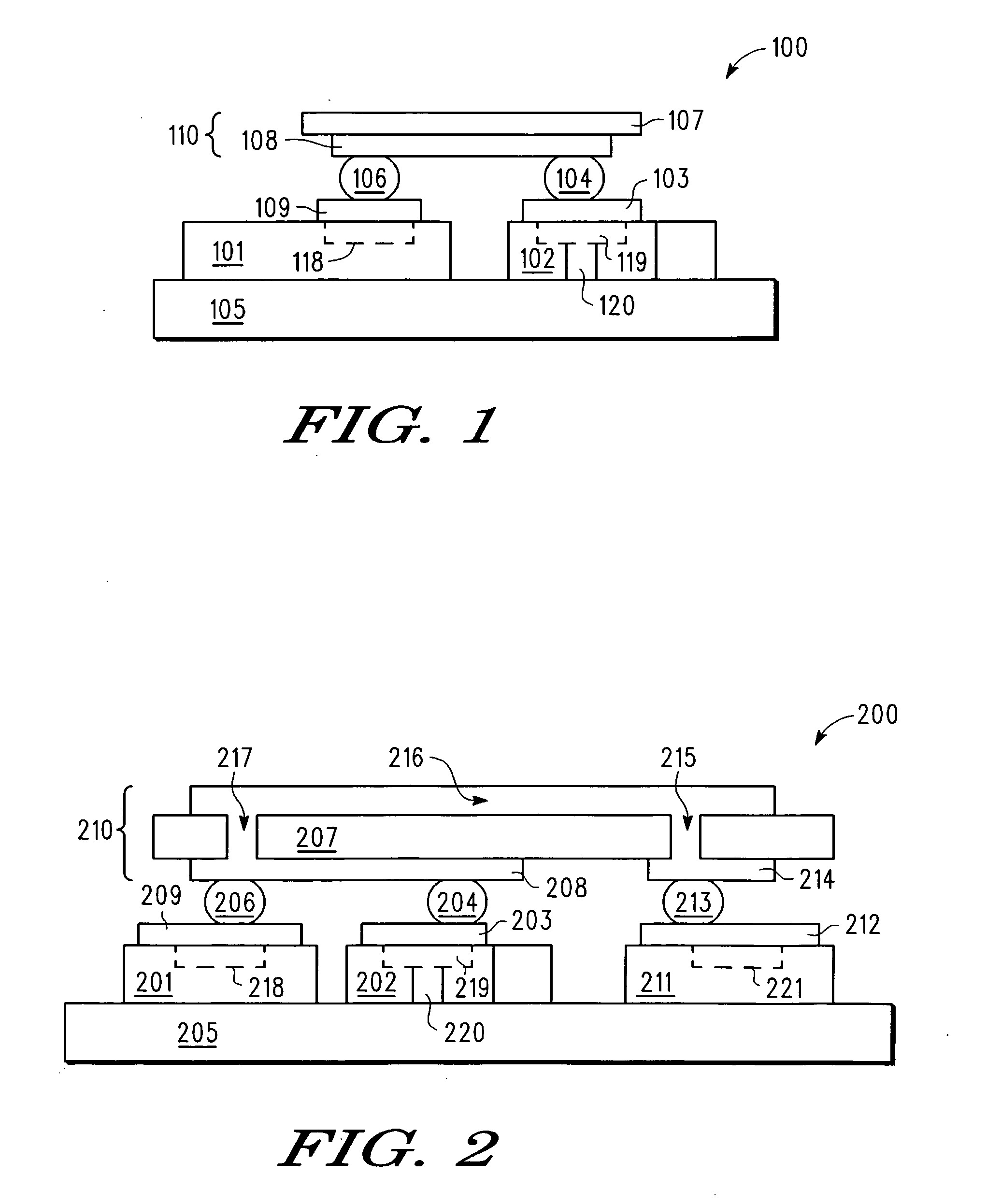
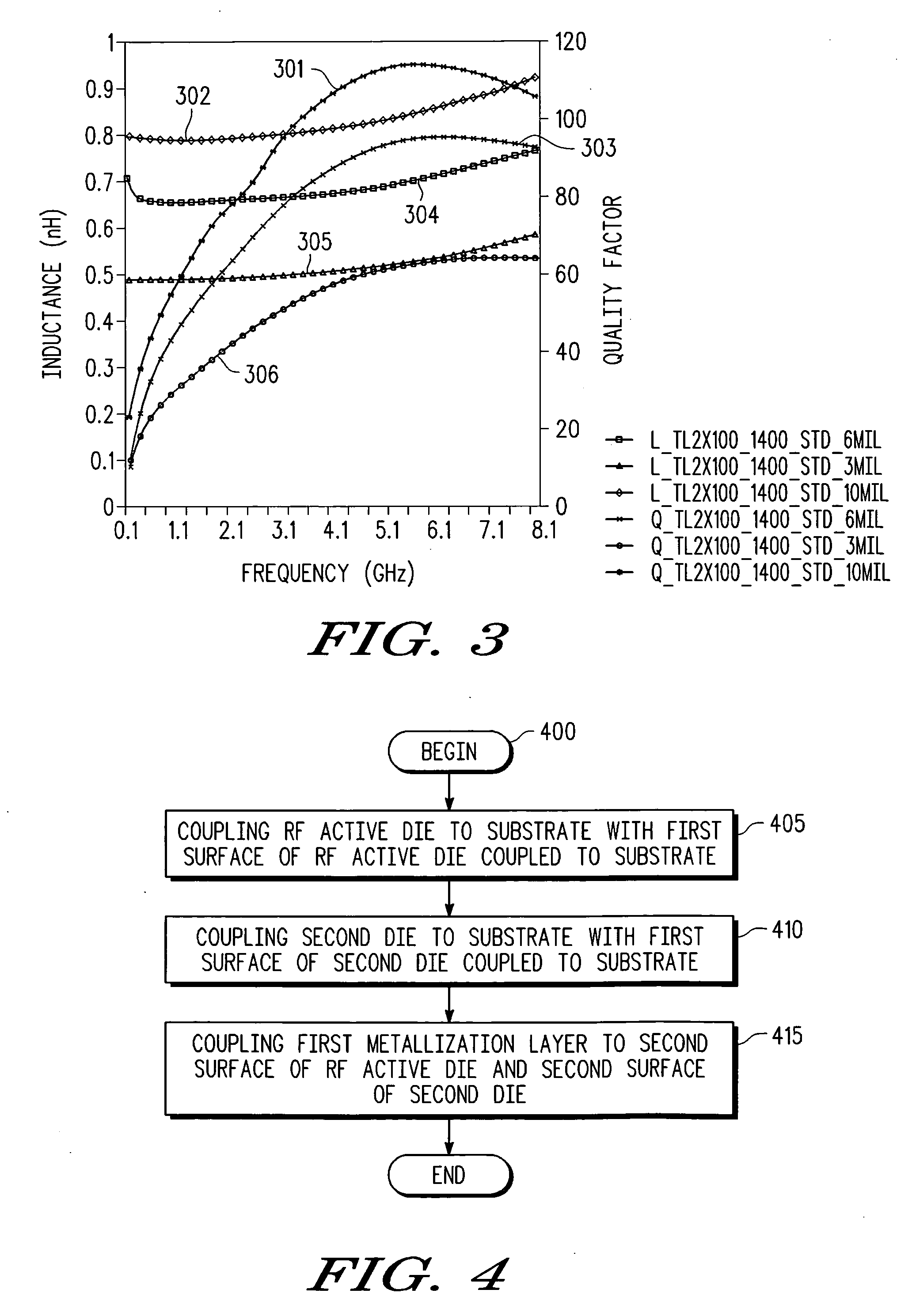
[0010]The following detailed description of the invention is merely exemplary in nature and is not intended to limit the invention or the application and uses of the invention. Furthermore, there is no intention to be bound by any theory presented in the preceding background of the invention or the following detailed description.

[0011]The invention may be described herein in terms of functional and / or schematic components. It should be appreciated that such components may be realized in any number of practical ways. For example, an embodiment of the invention may employ various elements, e.g., conductive traces, integrated passive devices, semiconductor substrate materials, dielectric materials, or the like, which may have characteristics or properties known to those skilled in the art. In addition, those skilled in the art will appreciate that the present invention may be practiced in conjunction with any number of practical circuit topologies and applications, and that the circuit...


PUM


Abstract

An integrated matching network and method for manufacturing an integrated matching network are provided. The method includes forming (405) a first die on a substrate, forming (410) a second die on the substrate, and forming (415) a metallization layer on the first and second dies. The second die has a capacitance, the metallization layer has an inductance, and the capacitance and inductance together provide a shunt impedance from the first die to the substrate. The integrated matching network includes a first die having a PA (101), a second die having a capacitor (102), and a metal interconnect (108) coupled to the PA and the first capacitor. The metal interconnect (108) has an inductance. The capacitor (102) and metal interconnect (108) form a shunt impedance.

Description

FIELD OF THE INVENTION[0001]The present invention generally relates to electronic devices that receive and transmit a signal and, more particularly, relates to methods and systems for integrating electronic devices for impedance matching.BACKGROUND OF THE INVENTION[0002]In many communication base stations, power amplifiers are used to boost the amplitude of relatively weak communication signals. These power amplifiers typically rely on matching circuits, which generally include capacitor and inductor elements, to match the impedances of the power amplifier to other radio components. Traditional integration of power amplifier (PA) matching network inductances at lower frequencies (e.g., less than or equal to about 2.0 GHz) involves the use of wirebonds, wherein the inductance is proportional to the wire length. With increasing frequencies, these inductances typically become smaller, and the control of wirebond length generally becomes more difficult. For example, as the inductance de...

Claims


Application Information

Patent Timeline
Patent Type & Authority Applications(United States)
IPC IPC(8): H01L29/80H01L23/48
CPCH01L23/66H01L25/0655H01L2223/6655H01L2924/19104H01L2924/0002H01L2924/3011H01L2924/00H01L2224/16227H01L2224/16235H01L2224/32245H01L2224/73253H01L2924/15192
Inventor MILLER, MELVY F.FOERSTNER, JUERGEN A.
Owner NXP USA INC
Why Eureka
Try Eureka