Memory device with emulated characteristics

a memory device and emulated technology, applied in the field of digital memory, can solve the problems of cost prohibitiveness of large-capacity memory modules in some systems, and the relationship between the capacity and the price of memory chips,

Inactive Publication Date: 2008-05-01
GOOGLE LLC
View PDF99 Cites 147 Cited by
  • Summary
  • Abstract
  • Description
  • Claims
  • Application Information

AI Technical Summary

Problems solved by technology

However, there is also an exponential relationship between a memory chip's capacity and its price.
As a result, large capacity memory modules may be cost prohibitive in some systems.

Method used


Image

  • Memory device with emulated characteristics
  • Memory device with emulated characteristics
  • Memory device with emulated characteristics

Examples


Embodiment Construction

[0029] The invention will be understood more fully from the detailed description given below and from the accompanying drawings of embodiments of the invention which, however, should not be taken to limit the invention to the specific embodiments described, but are for explanation and understanding only.

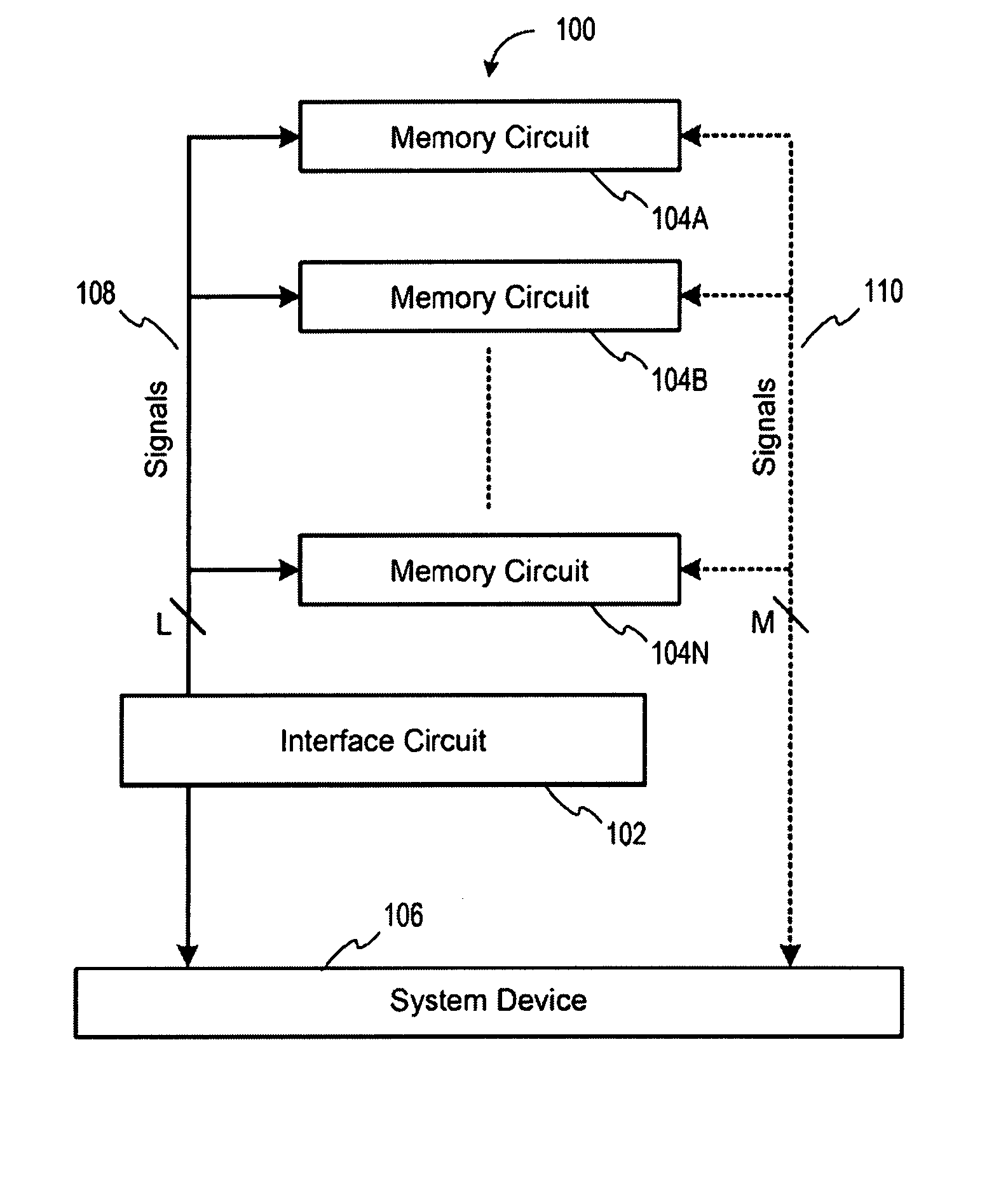
[0030]FIG. 1 illustrates a system 100 including a system device 106 coupled to an interface circuit 102, which is in turn coupled to a plurality of physical memory circuits 104A-N. The physical memory circuits may be any type of memory circuits. In some embodiments, each physical memory circuit is a separate memory chip. For example, each may be a DDR2 DRAM. In some embodiments, the memory circuits may be symmetrical, meaning each has the same capacity, type, speed, etc., while in other embodiments they may be asymmetrical. For ease of illustration only, three such memory circuits are shown, but actual embodiments may use any plural number of memory circuits. As will be discussed be...


PUM


Abstract

A memory subsystem is provided including an interface circuit adapted for communication with a system and a majority of address or control signals of a first number of memory circuits. The interface circuit includes emulation logic for emulating at least one memory circuit of a second number.

Description

RELATED APPLICATION [0001] This application is a continuation of commonly-assigned U.S. patent application Ser. No. 11 / 762,010 entitled “Memory Device with Emulated Characteristics” filed Jun. 12, 2007 by Rajan, et al., which, in turn, is a continuation-in-part of commonly-assigned U.S. patent application Ser. No. 11 / 461,420 entitled “System and Method for Simulating a Different Number of Memory Circuits” filed Jul. 31, 2006 by Rajan, et al., which are incorporated by reference as if fully set forth herein.BACKGROUND OF THE INVENTION [0002] 1. Technical Field of the Invention [0003] This invention relates generally to digital memory such as used in computers, and more specifically to organization and design of memory modules such as DIMMs. [0004] 2. Background Art [0005] Digital memories are utilized in a wide variety of electronic systems, such as personal computers, workstations, servers, consumer electronics, printers, televisions, and so forth. Digital memories are manufactured ...

Claims


Application Information

Patent Timeline
Patent Type & Authority Applications(United States)
IPC IPC(8): G06F9/455
CPCG06F13/4243G11C7/10G11C11/406G11C7/1072Y02B60/1228Y02B60/1235G11C11/40618Y02D10/00
Inventor RAJAN, SURESH NATARAJANSCHAKEL, KEITH R.SEBASTIAN SMITH, MICHAEL JOHNWANG, DAVID T.WEBER, FREDERICK DANIEL
Owner GOOGLE LLC
Why Eureka
Try Eureka