Flash memory device with multi-level cells and method of writing data therein

a flash memory device and multi-level cell technology, applied in the field of flash memory devices, can solve the problems of inability to adapt to the operation of the mlc flash memory device, and inability to write at the same tim

Active Publication Date: 2008-05-01
SAMSUNG ELECTRONICS CO LTD
View PDF4 Cites 386 Cited by
  • Summary
  • Abstract
  • Description
  • Claims
  • Application Information

AI Technical Summary

Problems solved by technology

When compared to SLC flash memory devices, MLC flash memory devices offer the advantage of increased storage capacity, but suffer the disadvantage of increased write times. In addition, there have been relatively recent proposals relating to hybrid NAND flash memories which selectively utilize memory cells in either MLC or SLC modes.
Conventionally mapping schemes, however, are generally unsuitable or inefficient for an MLC flash memory device.
In particular, writing speeds may not be desirable in the MLC flash memory device operable with conventional the log block mapping.

Method used


Image

  • Flash memory device with multi-level cells and method of writing data therein
  • Flash memory device with multi-level cells and method of writing data therein
  • Flash memory device with multi-level cells and method of writing data therein

Examples


Embodiment Construction

[0032]Preferred embodiments of the present invention will be described below in more detail with reference to the accompanying drawings. The present invention may, however, be embodied in different forms and should not be constructed as limited to the embodiments set forth herein. Rather, these embodiments are provided so that this disclosure will be thorough and complete, and will fully convey the scope of the present invention to those skilled in the art. Like reference numerals refer to like elements throughout the accompanying figures.

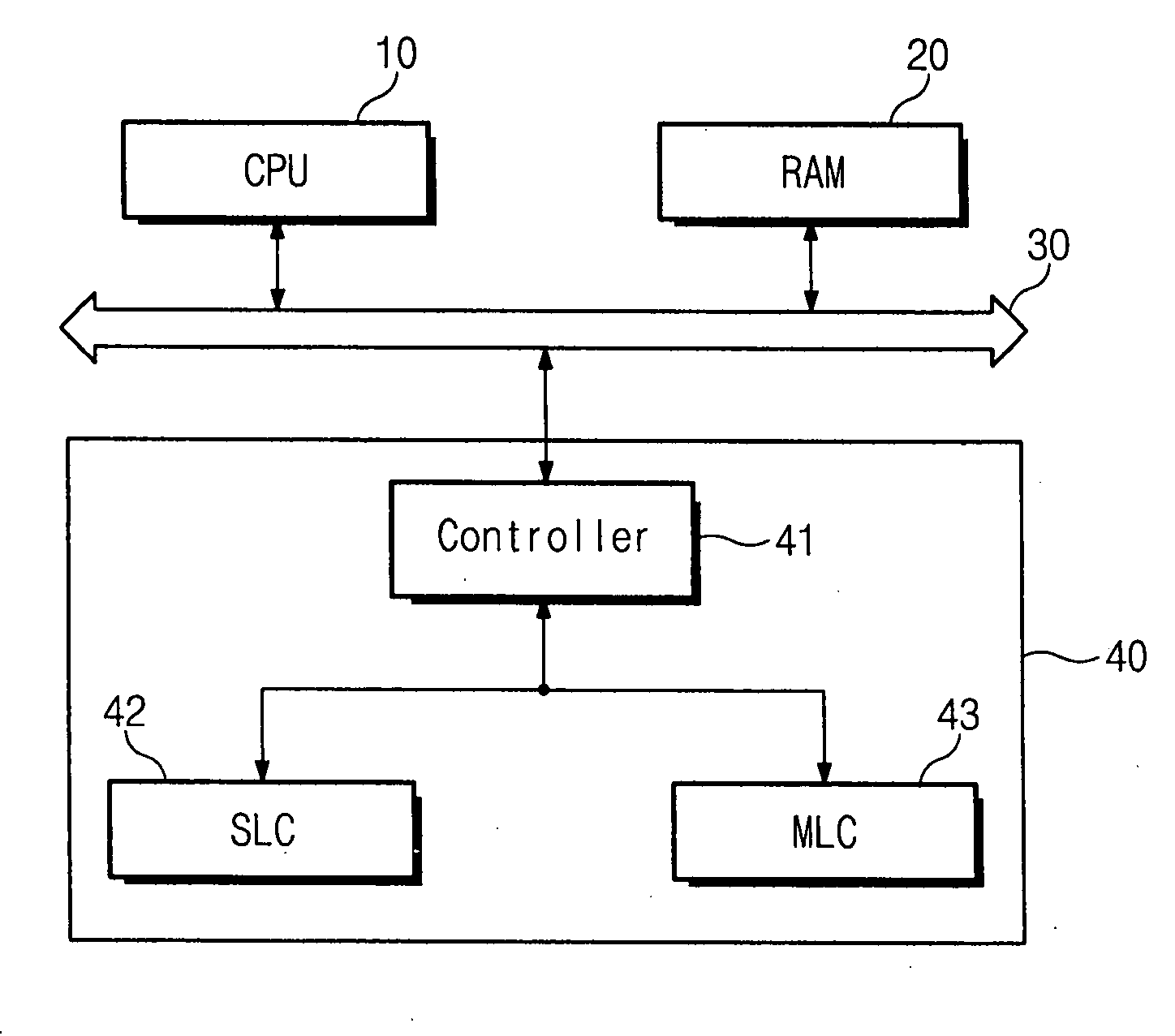
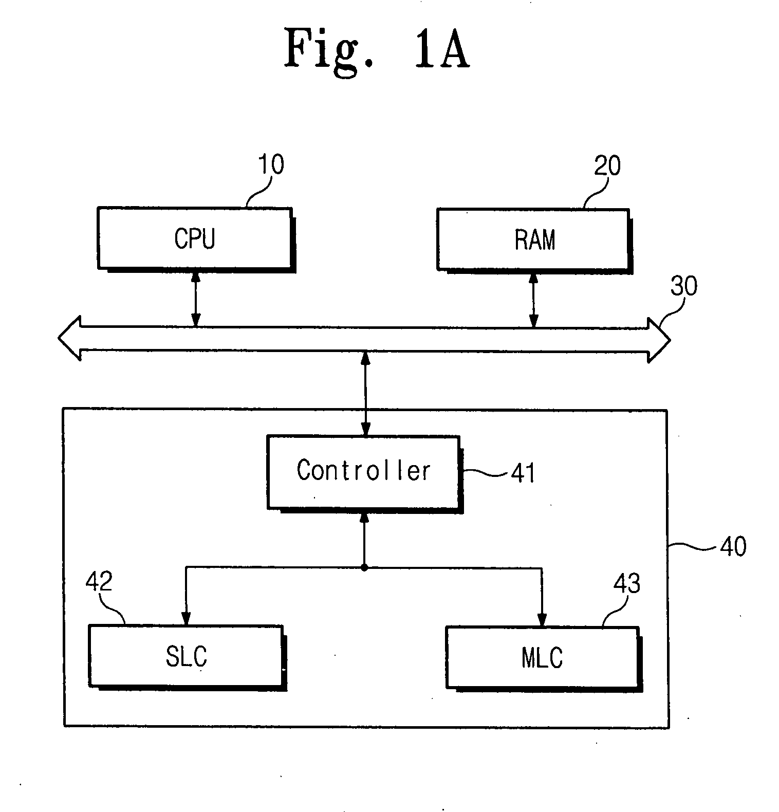
[0033]FIG. 1A is a block diagram illustrating a flash memory system which includes an SLC block and an MLC block according to an embodiment of the present invention. As shown, the system includes a central processing unit (CPU) 10, a random access memory (RAM) 20, a system bus 30, and a flash memory device 40. The flash memory device 40 includes a controller 41 which interfaces with the bus system 30, an SLC block 42, and an MLC block 43.

[0034]A lo...


PUM


Abstract

In one aspect, a method of writing data in a flash memory system is provided. The flash memory system forms an address mapping pattern according to a log block mapping scheme. The method includes determining a writing pattern of data to be written in a log block, and allocating one of SLC and MLC blocks to the log block in accordance with the writing pattern of the data.

Description

BACKGROUND[0001]The present invention generally relates to flash memory devices, and more particularly, the present invention relates to address mapping techniques for flash memory devices.[0002]A claim of priority under 35 U.S.C. §119 is made to Korean Patent Application No. 2006-105692, filed Oct. 30, 2006, the entire contents of which are hereby incorporated by reference.[0003]In an effort to increase storage capacity, flash memory devices have been developed in which each flash cell is capable of storing two or more bits. These types of multi-bit memory devices are typically referred to as “multi-level cell” or “MLC” devices. In contrast, flash memory devices storing 1-bit data per memory cell are typically referred to a “single-level cell” or “SLC” devices. When compared to SLC flash memory devices, MLC flash memory devices offer the advantage of increased storage capacity, but suffer the disadvantage of increased write times. In addition, there have been relatively recent prop...

Claims


Application Information

Patent Timeline
Patent Type & Authority Applications(United States)
IPC IPC(8): G06F12/06
CPCG06F2212/7208G11C2211/5641G06F12/0246G11C16/02G11C16/04G11C16/16G06F3/0613G06F3/0631G06F3/0632G06F3/064G06F3/0679G06F2212/1021G06F2212/2022G06F2212/7202
Inventor CHEON, WON-MOONKIM, SEON-TAEKPARK, CHAN-IKCHOI, SUNG-UP
Owner SAMSUNG ELECTRONICS CO LTD
Why Eureka
Try Eureka