Package designs for vertical conduction die

Inactive Publication Date: 2008-05-15
GEM SERVICES
View PDF26 Cites 20 Cited by
  • Summary
  • Abstract
  • Description
  • Claims
  • Application Information

AI Technical Summary

Benefits of technology

[0011]These and other embodiments of the present invention, as well as its features and some potent

Problems solved by technology

However, the low resistance per unit area exhibited by vertical conduction discretes devices (such as conventio

Method used


Image

  • Package designs for vertical conduction die
  • Package designs for vertical conduction die
  • Package designs for vertical conduction die

Examples


Embodiment Construction

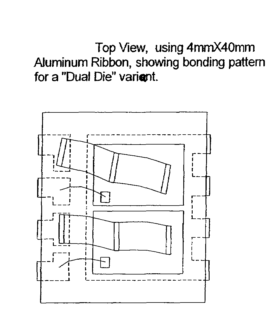
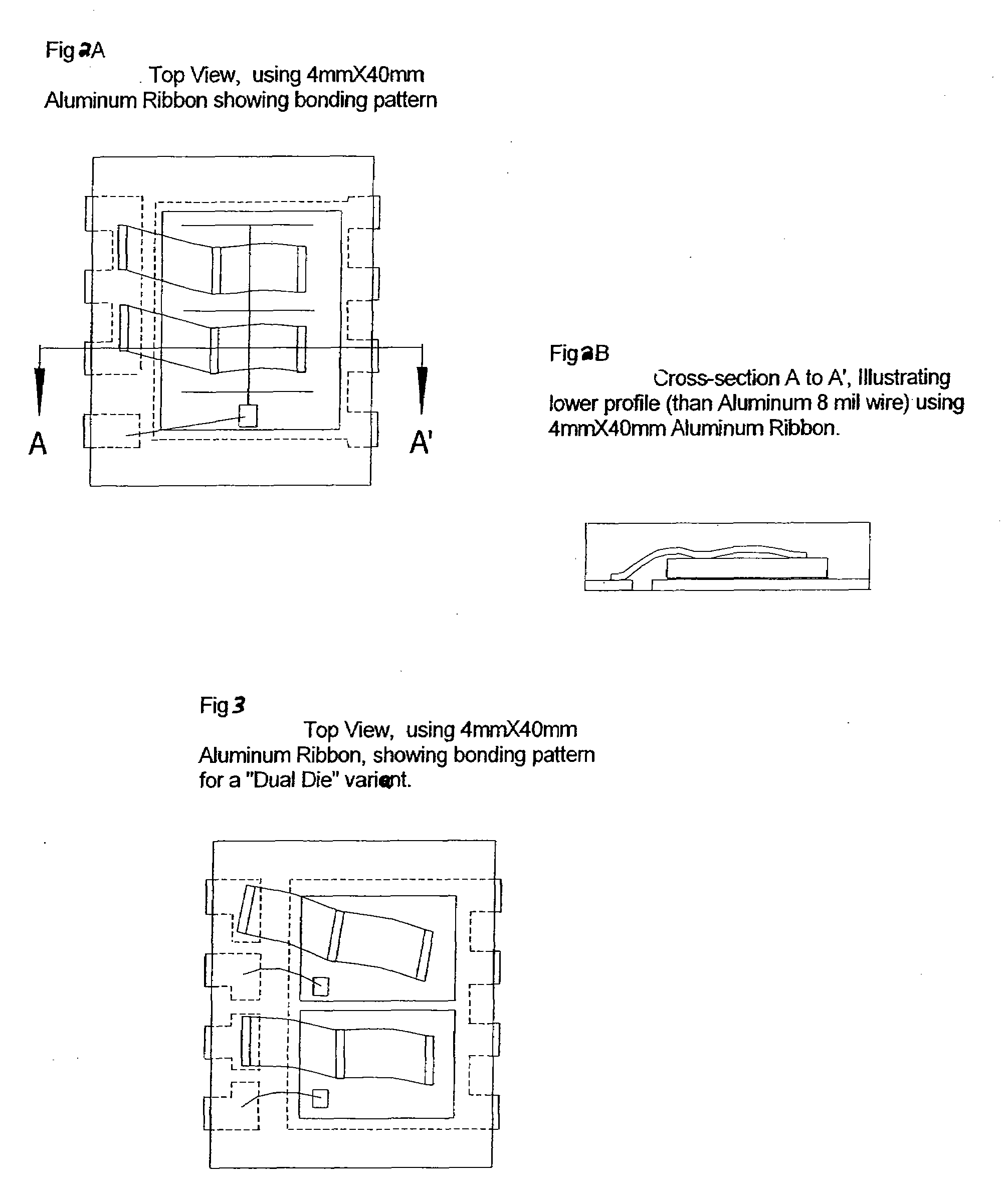
[0025]Device packages in accordance with certain embodiments of the present invention involve the use of Aluminum ribbons, rather than bond wires, to establish low resistance contacts with at least one surface of a vertical conduction die.

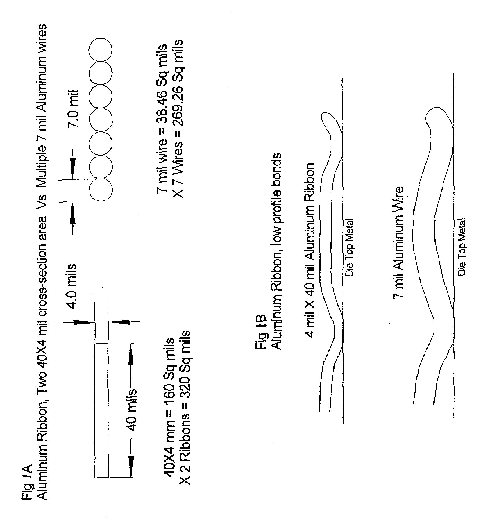
[0026]Orthodyne Electronics of Irvine, Calif., a leading manufacturer of Aluminum wire bonders, has recently released a series of machines that are capable of bonding Aluminum ribbons that vary in width and thickness from 20 mils wide×2 mils thick, up to 80 mils wide×10 mils thick. TABLE A lists the bond wire diameter cross section versus dimensions of electrically comparable Aluminum ribbons.

TABLE AWire Diameter5 mil8 mil10 mil12 mil14 mil15 mil16 mil20 milRIBBON20 × 2 mil2.00.80.50.40.30.20.20.120 × 3 mil3.11.20.80.50.40.30.30.230 × 3 mil4.61.81.10.80.60.50.40.340 × 4 mil8.13.22.01.41.00.90.80.540 × 6 mil12.24.83.12.11.61.41.20.860 × 6 mil18.37.24.63.22.32.01.81.160 × 8 mil24.49.56.14.23.12.72.41.580 × 6 mil24.49.56.14.23.12.72.41.580 × 8 mil32.6...


PUM


Abstract

Embodiments in accordance with the present invention relate to packaging designs for vertical conduction semiconductor devices which include low electrical resistance contacts with a top surface of the die. In one embodiment, the low resistance contact may be established by the use of Aluminum ribbon bonding with one side of a leadframe, or with both of opposite sides of a leadframe. In accordance with a particular embodiment, the vertical conduction device may be housed within a Quad Flat No-lead (QFN) package modified for that purpose.

Description

BACKGROUND OF THE INVENTION[0001]Widespread demand for “power management semiconductor products”, discrete, integrated, and combinations of technologies in very high volume portable consumer products (such as portable telecom, digital cameras, MP3 players, pocket computers, etc.), has spawned new products to generate and switch a host of voltages from batteries. The pressure of large volume production has in turn driven the rapid evolution of specialized semiconductor products, and given rise to successive generations of device packages exhibiting reduced vertical profiles, smaller footprints, lower thermal and electrical resistance, and cheaper manufacturing cost.[0002]Some acceptable alternatives exist for packages requiring only a single low resistance contact to one side of the housed die. An example of such a die having contact on only a single side includes an integrated circuits, a power integrated circuit (power ICs), and a lateral discrete.[0003]However, the low resistance ...

Claims


Application Information

Patent Timeline
IPC IPC(8): H01L23/495H01L21/00
CPCH01L23/4952H01L2924/12032H01L23/49541H01L23/49575H01L24/41H01L24/45H01L24/48H01L24/49H01L24/91H01L2224/45014H01L2224/45015H01L2224/45124H01L2224/45144H01L2224/45147H01L2224/48091H01L2224/48247H01L2224/4846H01L2224/4847H01L2224/48599H01L2224/48699H01L2224/4903H01L2224/49051H01L2224/49171H01L2924/01002H01L2924/01004H01L2924/01005H01L2924/01006H01L2924/01013H01L2924/01014H01L2924/01015H01L2924/01029H01L2924/01033H01L2924/01042H01L2924/01078H01L2924/01079H01L2924/01082H01L2924/13091H01L2924/14H01L2924/19043H01L2924/2076H01L2924/30107H01L2924/3011H01L23/49524H01L2224/73221H01L2224/48472H01L2924/00014H01L2924/00011H01L2924/00H01L2224/40245H01L2924/181H01L2224/05554H01L24/40H01L2224/40091H01L2224/0603H01L2224/37124H01L24/37H01L2224/49111H01L2924/00015H01L2924/00012H01L2224/37099H01L2224/85399H01L2224/05599H01L2924/206H01L2224/84
Inventor HARNDEN, JAMESCHIA, ANTHONYWONG, LIMINGYANG, HONGBO
Owner GEM SERVICES
Why Eureka
Try Eureka