Package design and method of manufacture for chip grid array

a technology of grid array and semiconductor chips, applied in the direction of semiconductor devices, semiconductor/solid-state device details, electrical apparatus, etc., can solve the problems of increasing the space required by each semiconductor chip, and reducing the size of the packag

Inactive Publication Date: 2005-08-16
ADVANPAK SOLUTIONS PTE
View PDF10 Cites 25 Cited by
  • Summary
  • Abstract
  • Description
  • Claims
  • Application Information

AI Technical Summary

Benefits of technology

[0021]The main objective of the invention is to provide a package design and method of fabrication for semiconductor chips that eliminates the need for a first level package. The package design should provide reliable interconnections to the chip and to the next level of package. In addition it needs to protect the semiconductor chip and the interconnections from the environment.
[0026]An embodiment of the present invention is shown in FIG. 2. The semiconductor chip 20 with conductive pillars 22 and solder balls 24 is encapsulated in a molding compound 26. A bottom view is shown in FIG. 2A. The bottom side of the semiconductor chip is exposed to allow for the attachment of a heat sink 28 as shown in FIG. 3. The package has a fully encapsulated or molded semiconductor chip and provides a CGA for interconnect to the next level of package while eliminating the need for a substrate or interposer.

Problems solved by technology

The inclusion of enclosures for environmental protection results in larger packages with larger distances between semiconductor chips and thereby longer signal delays.
Inherent in these designs is that the peripheral leads increase the space required by each semiconductor chip.
Again this increase in chip spacing results in longer signal delays.
Alpha particles emitted from solder alloys used as interconnects in BGA designs, have been shown to cause semiconductor devices to malfunction.
Although this design satisfies the criteria set above it has the disadvantage of increasing the area required by the semiconductor chip by 4x˜9x, due to the use of the interposer, or first level package.

Method used


Image

  • Package design and method of manufacture for chip grid array
  • Package design and method of manufacture for chip grid array
  • Package design and method of manufacture for chip grid array

Examples


Embodiment Construction

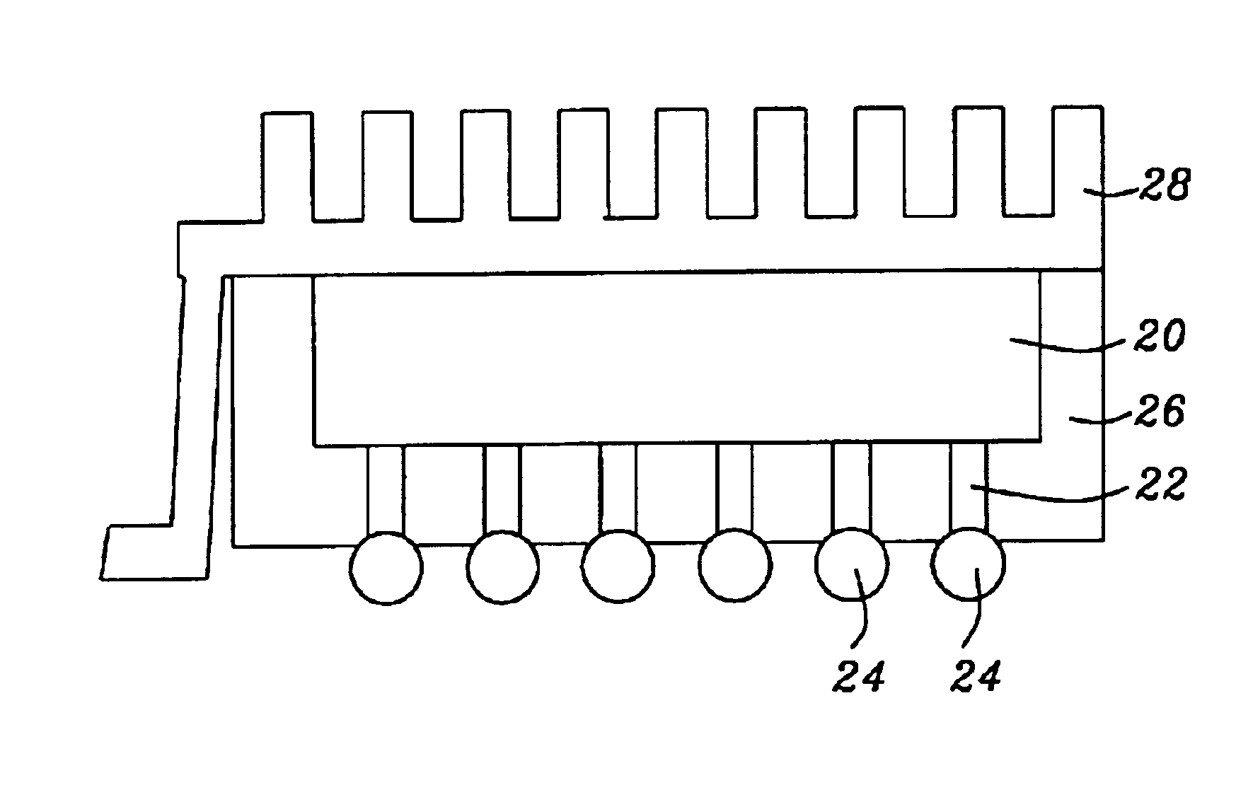
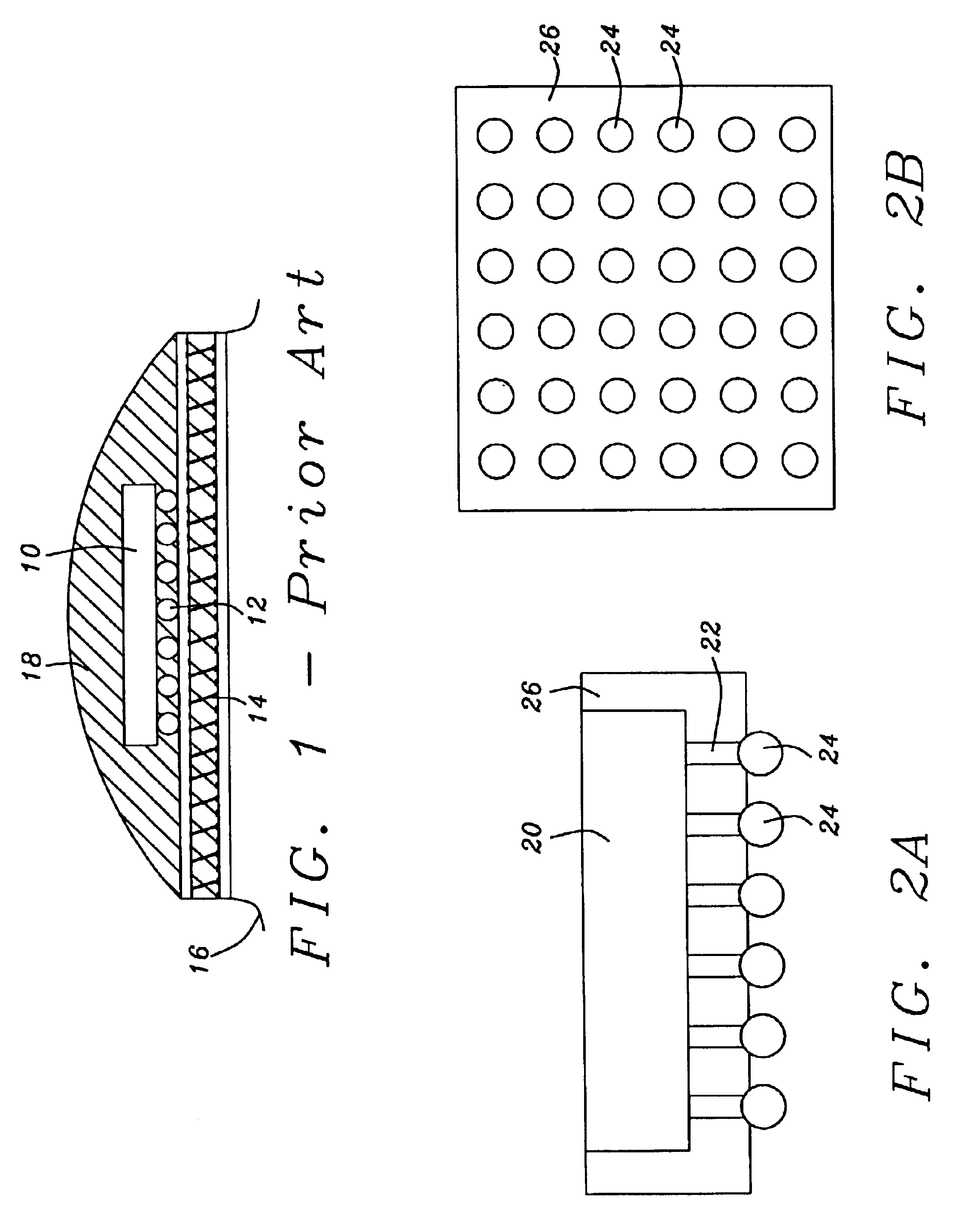
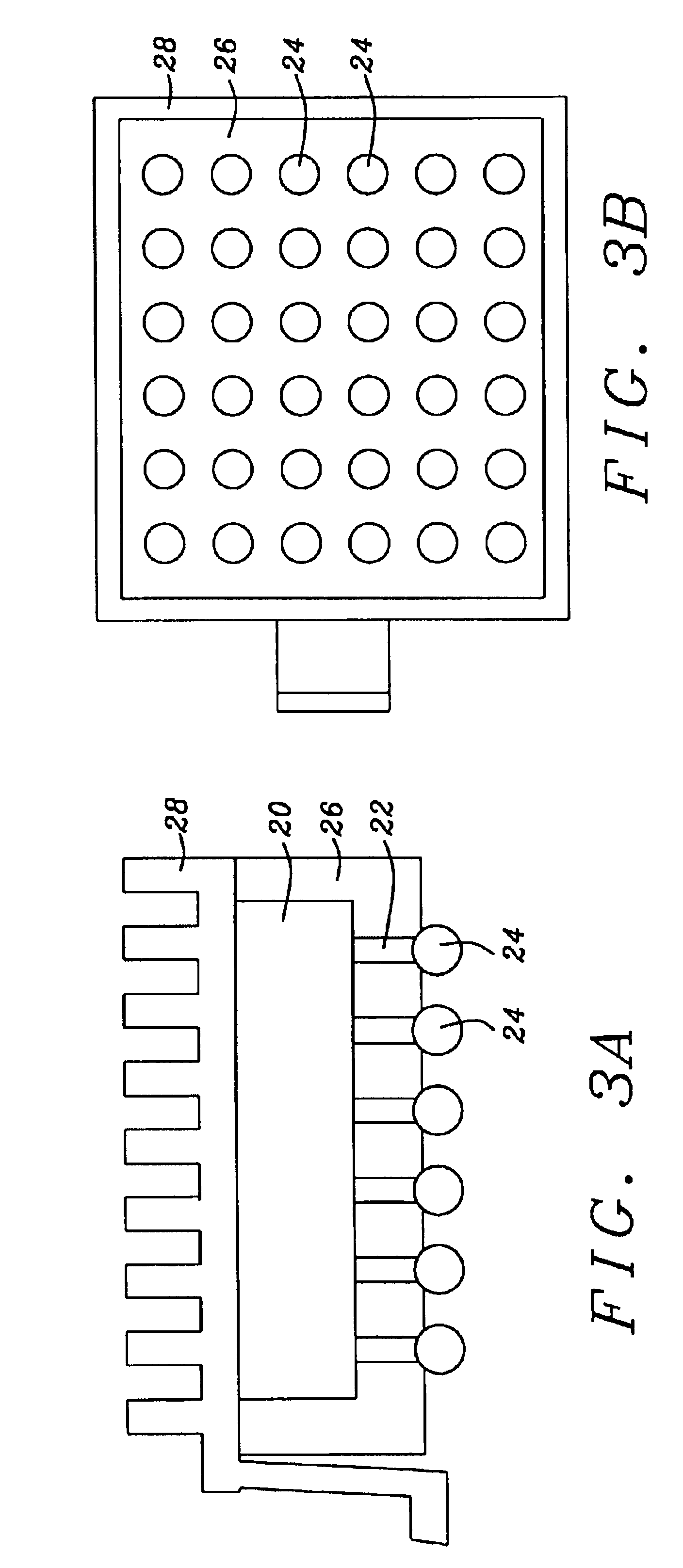
[0039]The decrease in semiconductor device sizes has resulted in VLSI integrated circuit chips with a large number of circuits per chip. The increase in circuits per chip has resulted in increased demand for interconnections to the chip. In order to meet the demand for the higher number of interconnections the use of BGA interconnection technology is being used extensively. BGA or solder ball technology has shown it can provide the high interconnection density required by allowing for close spacing of the interconnects as well as utilizing the total area of the semiconductor chip.

[0040]The new micron sized devices have been shown to be susceptible to alpha particle emissions that cause significant errors. Lead and lead alloys emit small amounts of alpha particles. In order to minimize the deleterious effects of the alpha particles copper pillars have been used. See U.S. Patent Application Publication U.S. Ser. No. 2002 / 0033412A1 herein incorporated by reference. The pillars displace...


PUM


Abstract

A chip level package utilizing a CGA is described. A semiconductor chip with pillars is molded in an encapsulant. Solder balls are added and connected to the chip pillars. The final package does not require a first level substrate or interposer and is able to be assembled to the next level as is. An additional embodiment describes the addition of a thermal heat sink to the packaged chip.

Description

RELATED PATENT APPLICATION[0001]This application is related to Ser. No. 10 / 236,385, filing date Sep. 6, 2002, now U.S. Pat. No. 6,734,039, issued May 11, 2004, assigned to a common assignee.BACKGROUND OF THE INVENTION[0002]1. Field of the Invention[0003]This invention relates in general to the design and method of manufacture of packages for semiconductor chips, and the input, output (I / O), interconnections to the chips, and more specifically to a semiconductor package that utilizes a method of manufacture, molding an encapsulant that encapsulates the semiconductor chip but allows the interconnections and the backside of the semiconductor chip to be free of encapsulant.[0004]2. Description of the Related Art[0005]The following three U.S. patents and one U.S. patent application relate to semiconductor chip packaging designs.[0006]U.S. Pat. No. 5,994,773 dated Nov. 30, 1999, issued to T. Hirakawa describes a BGA package incorporating a semiconductor chip and a printed circuit interpos...

Claims


Application Information

Patent Timeline
Patent Type & Authority Patents(United States)
IPC IPC(8): H01L23/34H01L23/31H01L23/28H01L23/36
CPCH01L23/3114H01L23/36H01L2224/16H01L2224/05573H01L21/568H01L24/96H01L2224/12105H01L2924/18162H01L2224/06131H01L2224/05647H01L2924/00014
Inventor HWEE, TAN KIMPEREZ, ROMANLAU, KEE KWANGCHEW, ALEXDIMAANO, ANTONIO
Owner ADVANPAK SOLUTIONS PTE
Why Eureka
Try Eureka