Radiation beam pulse trimming

a technology of beam pulse and beam beam, which is applied in the field of radiation system, can solve the problems of short life of materials at 193 nm, material transmission poor, and inability to rely on control algorithms

Inactive Publication Date: 2008-05-15
ASML NETHERLANDS BV
View PDF28 Cites 2 Cited by
  • Summary
  • Abstract
  • Description
  • Claims
  • Application Information

AI Technical Summary

Problems solved by technology

Thus, it is no longer possible to rely on a control algorithms that compensate for deviations of previous pulses and the averaging effect over the amount of pulses in the exposure because they are no longer applicable.
The problem is that these materials are not very effective at the smaller and smaller wavelengths being used today in lithography systems to form smaller and smaller elements.
For example, at wavelengths of 193 nm and below these materials exhibit poor transmission and / or have a short lifetime at 193 nm.

Method used


Image

  • Radiation beam pulse trimming
  • Radiation beam pulse trimming
  • Radiation beam pulse trimming

Examples


Embodiment Construction

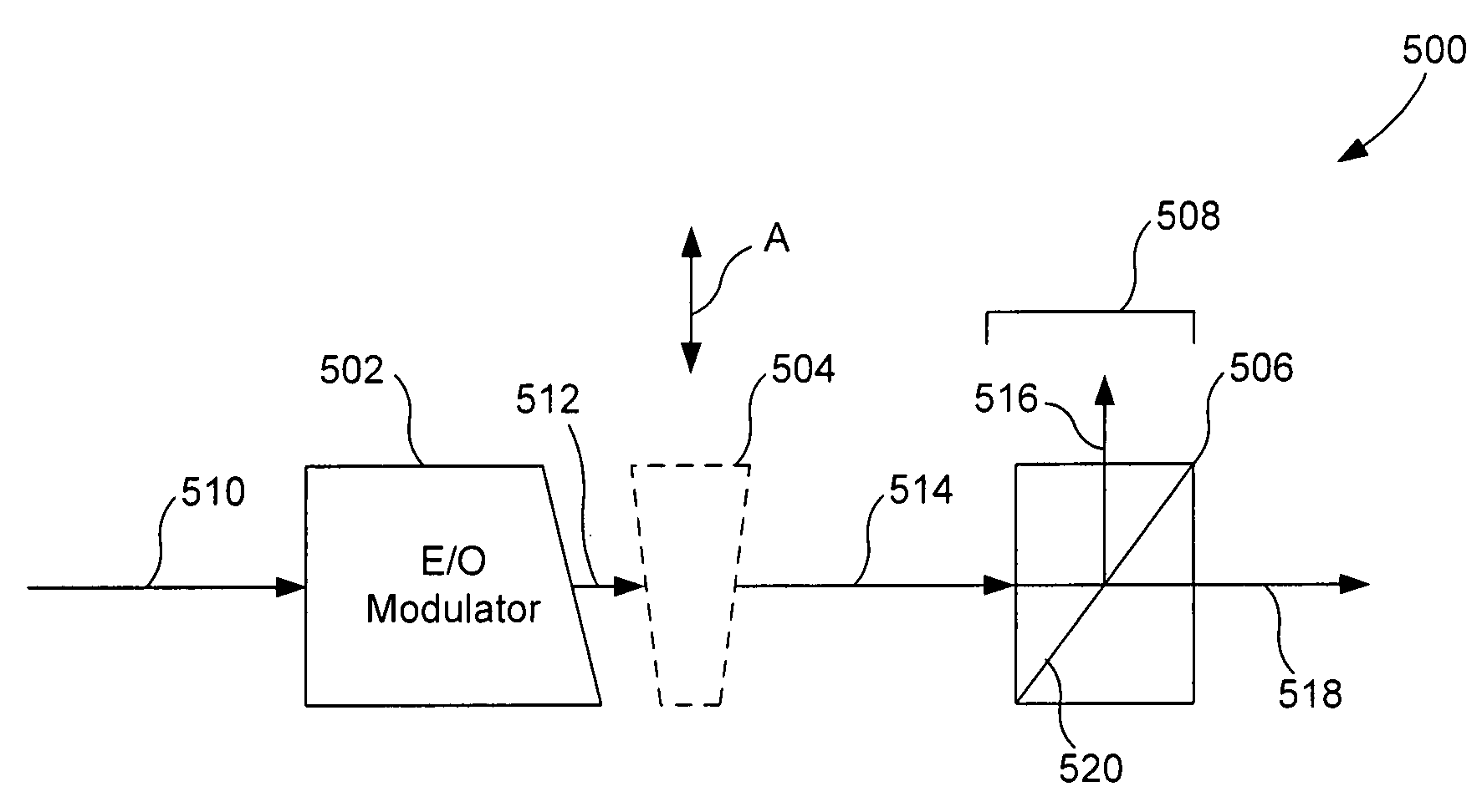
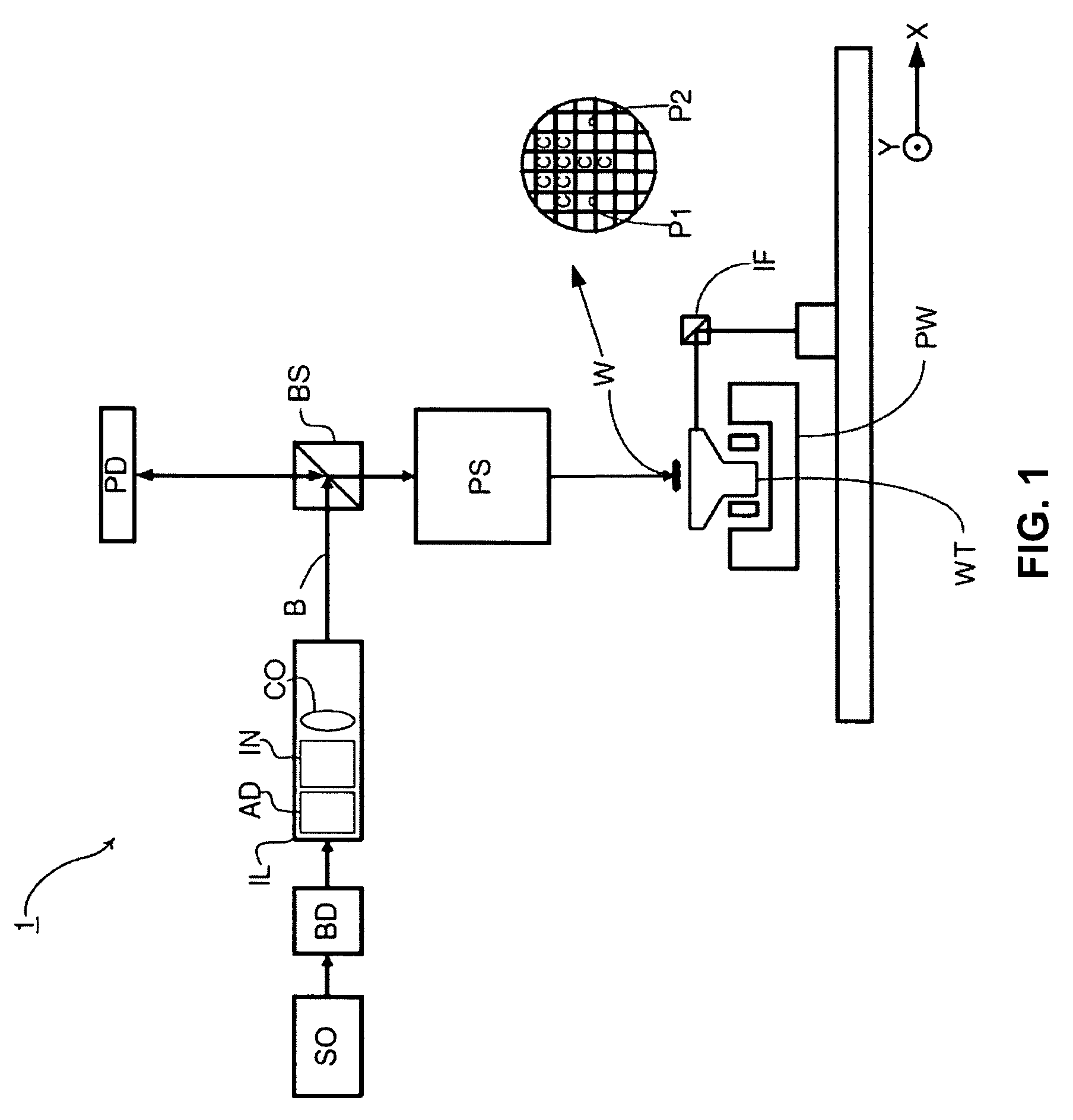
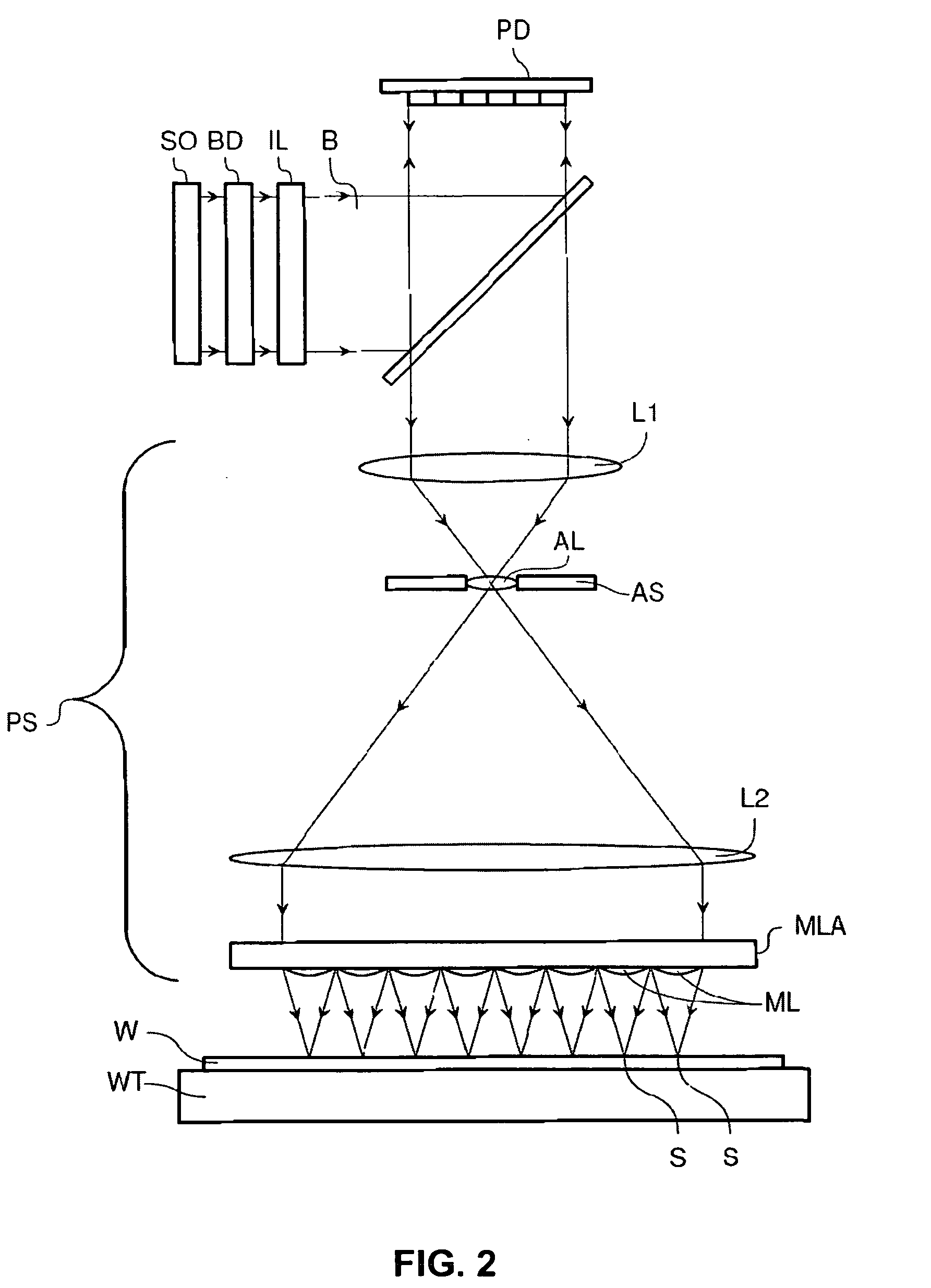
[0028]This specification discloses one or more embodiments that incorporate the features of this invention. The disclosed embodiment(s) merely exemplify the invention. The scope of the invention is not limited to the disclosed embodiment(s). The invention is defined by the claims appended hereto.

[0029]The embodiment(s) described, and references in the specification to “one embodiment”, “an embodiment”, “an example embodiment”, etc., indicate that the embodiment(s) described may include a particular feature, structure, or characteristic, but every embodiment may not necessarily include the particular feature, structure, or characteristic. Moreover, such phrases are not necessarily referring to the same embodiment. Further, when a particular feature, structure, or characteristic is described in connection with an embodiment, it is understood that it is within the knowledge of one skilled in the art to effect such feature, structure, or characteristic in connection with other embodimen...


PUM

PropertyMeasurementUnit
wavelengthaaaaaaaaaa
wavelengthsaaaaaaaaaa
diameteraaaaaaaaaa

Abstract

A system is used to perform fast and slow applications, for example fast application can be pulse trimming. The system includes a radiation source, an electro-optical modulator, and a beam splitter. The radiation source is configured to generate a polarized beam of radiation. The electro-optical modulator, formed of crystalline quartz, is configured to modulate the beam of radiation. The beam splitter is configured to direct a first portion of the beam to a beam dump and to form an output beam from a second portion of the beam.

Description

BACKGROUND[0001]1. Field of the Invention[0002]The present invention relates to radiation systems.[0003]2. Related Art[0004]A lithographic apparatus is a machine that applies a desired pattern onto a substrate or part of a substrate. A lithographic apparatus can be used, for example, in the manufacture of flat panel displays, integrated circuits (ICs) and other devices involving fine structures. In a conventional apparatus, a patterning device, which can be referred to as a mask or a reticle, can be used to generate a circuit pattern corresponding to an individual layer of a flat panel display (or other device). This pattern can be transferred onto all or part of the substrate (e.g., a glass plate), by imaging onto a layer of radiation-sensitive material (e.g., resist) provided on the substrate.[0005]Instead of a circuit pattern, the patterning device can be used to generate other patterns, for example a color filter pattern or a matrix of dots. Instead of a mask, the patterning dev...

Claims


Application Information

Patent Timeline
Patent Type & Authority Applications(United States)
IPC IPC(8): G02F1/01G02F1/00
CPCG03F7/70558G03F7/70041
Inventor NOORDMAN, OSCAR FRANCISCUS JOZEPHUSVINK, HENRI JOHANNES PETRUSVISSER, HUIBERT
Owner ASML NETHERLANDS BV
Why Eureka
Try Eureka