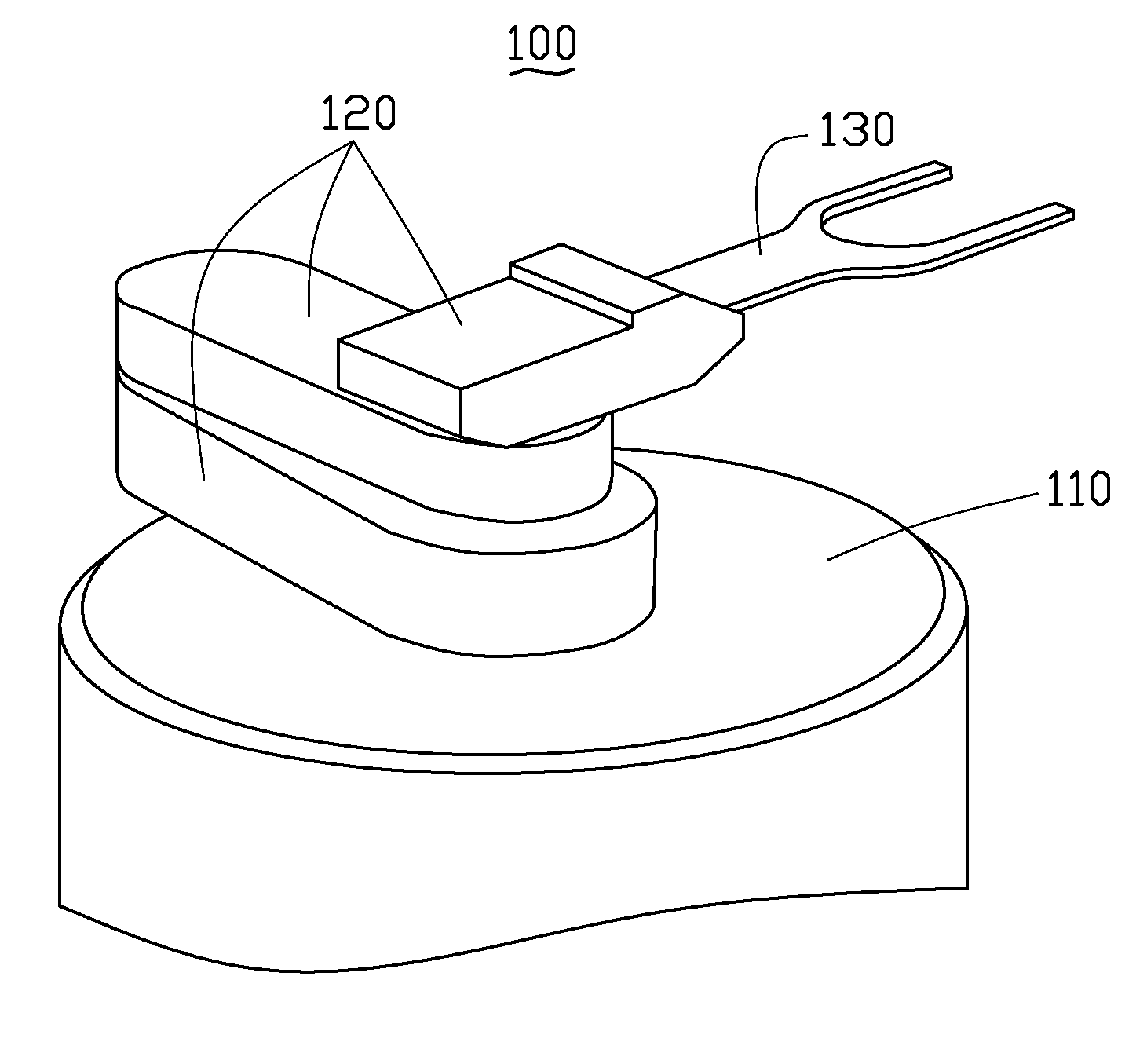
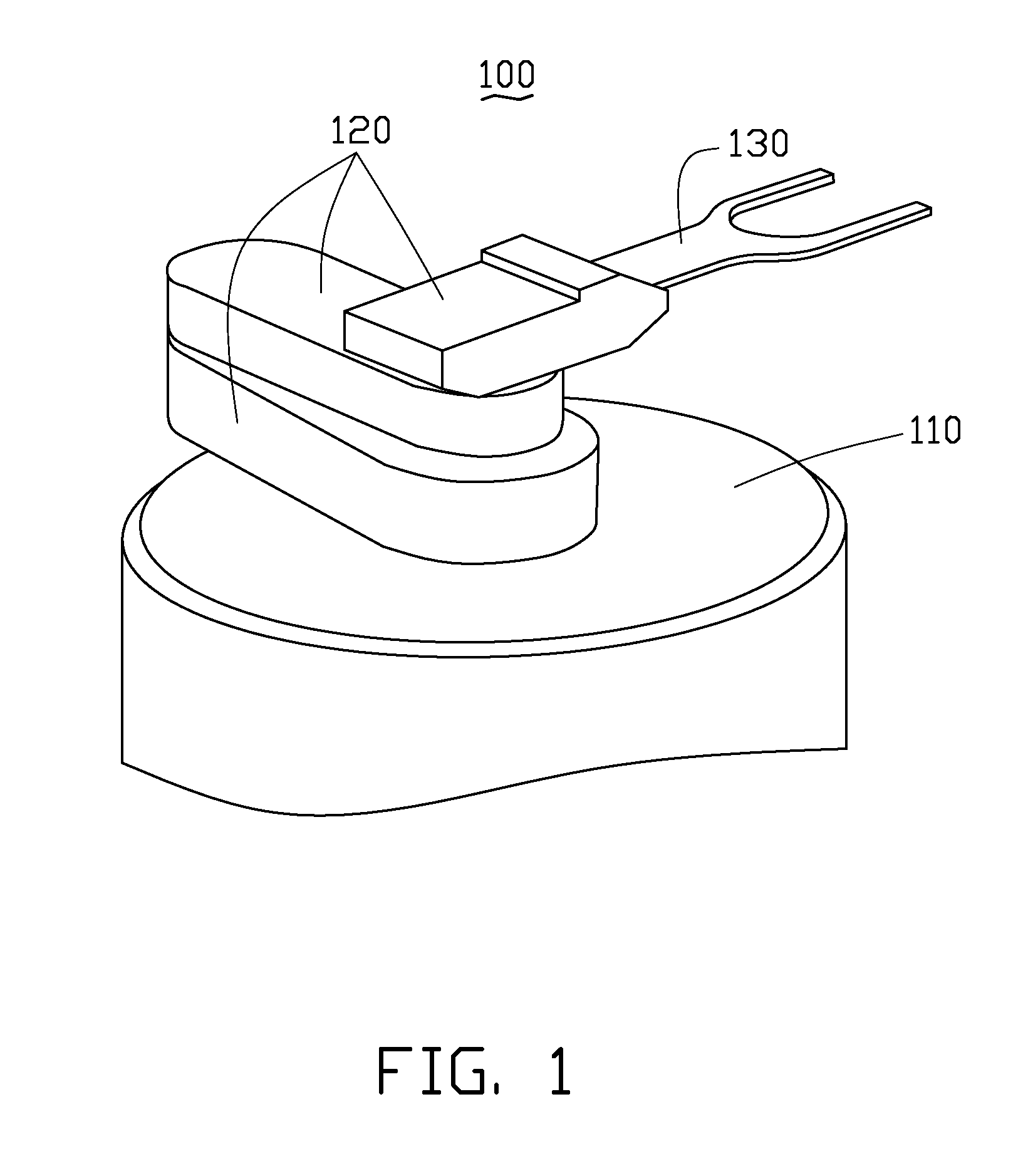
Transfer robot

a robot and robot technology, applied in the field of robots, can solve the problems of inability to accurately estimate whether the center of the silicon wafer has been displaced, etc., and achieve the effect of avoiding damage to the silicon wafer in the transfer process

Inactive Publication Date: 2008-05-22
FOXSEMICON INTEGRATED TECH INC
View PDF8 Cites 22 Cited by
  • Summary
  • Abstract
  • Description
  • Claims
  • Application Information

AI Technical Summary

Benefits of technology

[0009]The present transfer robot and method employ a plurality of optical sensors to accurately ascertain the actual horizontal location of the center of the silicon wafer and estimate whether the actual horizontal location of the center of the silicon wafer is displaced, and employ a plurality of displacement sensors to accurately ascertain the vertical position and the leveling of the silicon wafer and estimate whether the vertical position and / or leveling of the silicon wafer is displaced. Therefore, the present transfer robot can efficiently avoid damaging the silicon wafer in transfer.

Problems solved by technology

During transfer, if the centers or the vertical position or the leveling of the silicon wafers are displaced, the silicon wafers may be damaged or dragged.
However, the silicon wafer usually has a notch, and the conventional transfer robot is often influenced by the notch and is unable to accurately estimate whether the center of the silicon wafer has been displaced.
Furthermore, the conventional transfer robot cannot detect the leveling of the silicon wafer such that the silicon wafer may easily impact with other objects, etc., and may be damaged during transfer.

Method used


Image

  • Transfer robot
  • Transfer robot
  • Transfer robot

Examples


example 1

[0039]A method for transferring a silicon wafer 300 on an aligner 200 is provided.

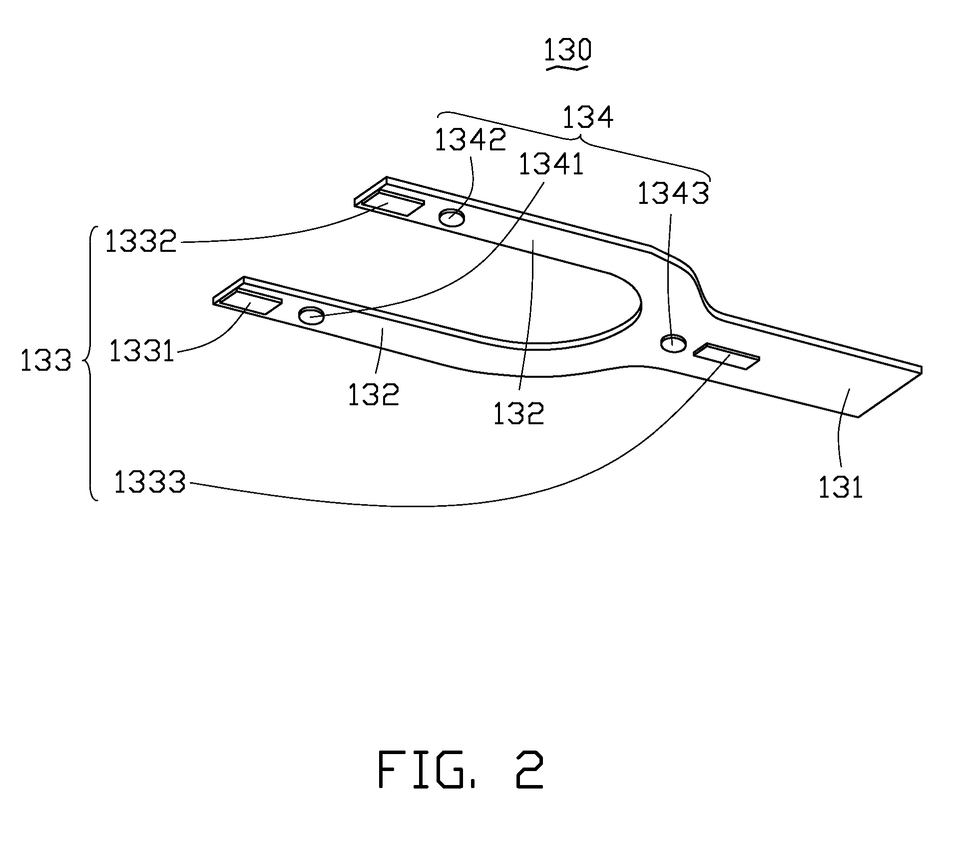
[0040]Referring to FIG. 4, a coordinate system is created with an initial position of the transfer robot 100 as an origin. The end-effector 130 of the transfer robot 100 begins to move. When the pair of first linear optical sensors 1331, 1332 are detected or reflected for the first time by two points 211, 212 at the periphery of the aligner 200, the two points 211, 212 are denoted as first reference points and the pair of first linear optical sensors 1331, 1332 sense the two first reference points 211, 212 to obtain information thereof and feedback the information into the micro processing unit of the base support 110. The micro processing unit calculates the center of the aligner 200 based on the information of the first reference point 211, 212 and known standard of the aligner 200, and the calculated center of the aligner 200 is a desired horizontal location of the center of the silicon wafer 300 if...

example 2

[0049]A method for transferring silicon wafers 1 to 25 in a cassette 500 is provided.

[0050]The method of example 2 is similar to that of example 1. Referring to FIG. 10, the silicon wafers 1 to 25 are placed in the cassette 500. The pair of first linear optical sensors 1331, 1332 are used to sense the periphery of the cassette 500. When the pair of first linear optical sensors 1331, 1332 are detected or reflected for the first time by two point 511, 512 of the periphery of the cassette 500, the two point 511, 512 are designed as first reference points and the pair of first linear optical sensors 1331, 1332 sense the two first reference points 511, 512 to obtain information thereof and feedback the information into the micro processing unit. The micro processing unit calculates the desired horizontal location of the centers of each of the silicon wafers 1 to 25 based on the first reference point 511, 512 and the known standard of the cassette 500.

[0051]Referring to FIG. 11, at least ...

example 3

[0054]A method for transferring a silicon wafer 700 on a process station or a buffer station is provided.

[0055]The method of example 3 is similar to that of example 1. Referring to FIGS. 13 to 16, the silicon wafer 700 should be placed in the process station 600. Referring to FIG. 13, the process station 600 includes a gate 610 configured (i.e., structured and arranged) for inserting the end-effector 130 into the process station 600, and two supporting block 620, 630 configured for placing the silicon wafer 700.

[0056]Referring to FIG. 14, the pair of first linear optical sensors 1331, 1332 are used to sense the periphery of the gate 610 of the process station 600. When the pair of first linear optical sensors 1331, 1332 are detected or reflected for the first time by two point 611, 612 of the periphery of the gate 610, the two point 611, 612 are designed as first reference points to calculates the desired horizontal location of the center of the silicon wafer 700 based on the known ...


PUM


Abstract

A transfer robot (100) for transferring a silicon wafer includes a base support (110), an end-effector (130) having a main body (131) and two spaced fingers (132) extending from the main body, an articulated arm (120) assembly interconnecting the base support and the end-effector, a pair of first linear optical sensors (1331, 1332) arranged on the respective fingers of the end-effector, a second linear optical sensor (1333) arranged on the main body of the end-effector, and a plurality of displacement sensors (134) arranged non-collinearly on the end-effector, for ascertaining a vertical position and a leveling of the silicon wafer. The first and second linear optical sensors are arranged non-collinearly on the end-effector for ascertaining a center of the silicon wafer.

Description

BACKGROUND OF THE INVENTION[0001]1. Field of the Invention[0002]The present invention relates to transfer robot and, more particularly, to a transfer robot with an automatic calibration function.[0003]2. Description of Related Art[0004]In the fabrication of semiconductors, silicon wafers are usually held in a storage cassette and then moved to various process stations by a transfer system. The transfer system must be able to precisely pick up the silicon wafers from the storage cassette and then precisely transfer them to a designated process station or a plurality of process stations where the silicon wafers undergoes some processes, such as heating or alignment. During transfer, if the centers or the vertical position or the leveling of the silicon wafers are displaced, the silicon wafers may be damaged or dragged.[0005]A conventional transfer robot with an automatic calibration function is used to detect the actual position of a silicon wafer and estimate whether the center of th...

Claims


Application Information

Patent Timeline
Patent Type & Authority Applications(United States)
IPC IPC(8): H01L21/68G06F19/00
CPCB25J9/1692B25J9/1697H01L21/68707G05B2219/45054H01L21/67265B65G47/905
Inventor HUANG, HUNG-KAICHENG, KAI-JEN
Owner FOXSEMICON INTEGRATED TECH INC
Why Eureka
Try Eureka