Optical preforms for solid state light emitting dice, and methods and systems for fabricating and assembling same

a technology of optical preforms and dice, which is applied in the direction of semiconductor/solid-state device manufacturing, semiconductor devices, electrical devices, etc., can solve the problems of increased manufacturing cost, time and/or yield, and achieve the effect of increasing manufacturing cost, time and/or yield, and high-efficiency optical processing of ligh

Inactive Publication Date: 2008-05-29
CREE INC
View PDF23 Cites 137 Cited by
  • Summary
  • Abstract
  • Description
  • Claims
  • Application Information

AI Technical Summary

Benefits of technology

[0006]Solid state light emitting devices according to some embodiments of the present invention comprise a solid state light emitting die that is configured to emit light upon energization thereof, and a preform that is configured to allow at least some light that is emitted from the solid state light emitting die to pass therethrough. A layer attaches and optically couples the preform and the solid state light emitting die to one another. An optical element is provided in and / or on the preform that is configured to modify at least some of the light that is emitted from the solid state light emitting die. By using a preform that is attached and optically coupled to the solid state light emitting die itself, high efficiency optical processing of the light emitted from the solid state light emitted die may be provided. Moreover, the preform may be fabricated using conventional microelectronic manufacturing techniques, and may be placed on the solid state light emitting die using conventional “pick and place” techniques, so that manufacturing cost, time and / or yield may be increased. In some embodiments, the layer adhesively attaches the preform and the solid state light emitting die to one another.

Problems solved by technology

Moreover, the preform may be fabricated using conventional microelectronic manufacturing techniques, and may be placed on the solid state light emitting die using conventional “pick and place” techniques, so that manufacturing cost, time and / or yield may be increased.

Method used


Image

  • Optical preforms for solid state light emitting dice, and methods and systems for fabricating and assembling same
  • Optical preforms for solid state light emitting dice, and methods and systems for fabricating and assembling same
  • Optical preforms for solid state light emitting dice, and methods and systems for fabricating and assembling same

Examples


Embodiment Construction

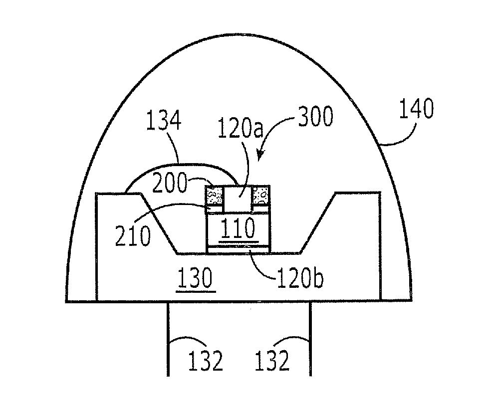
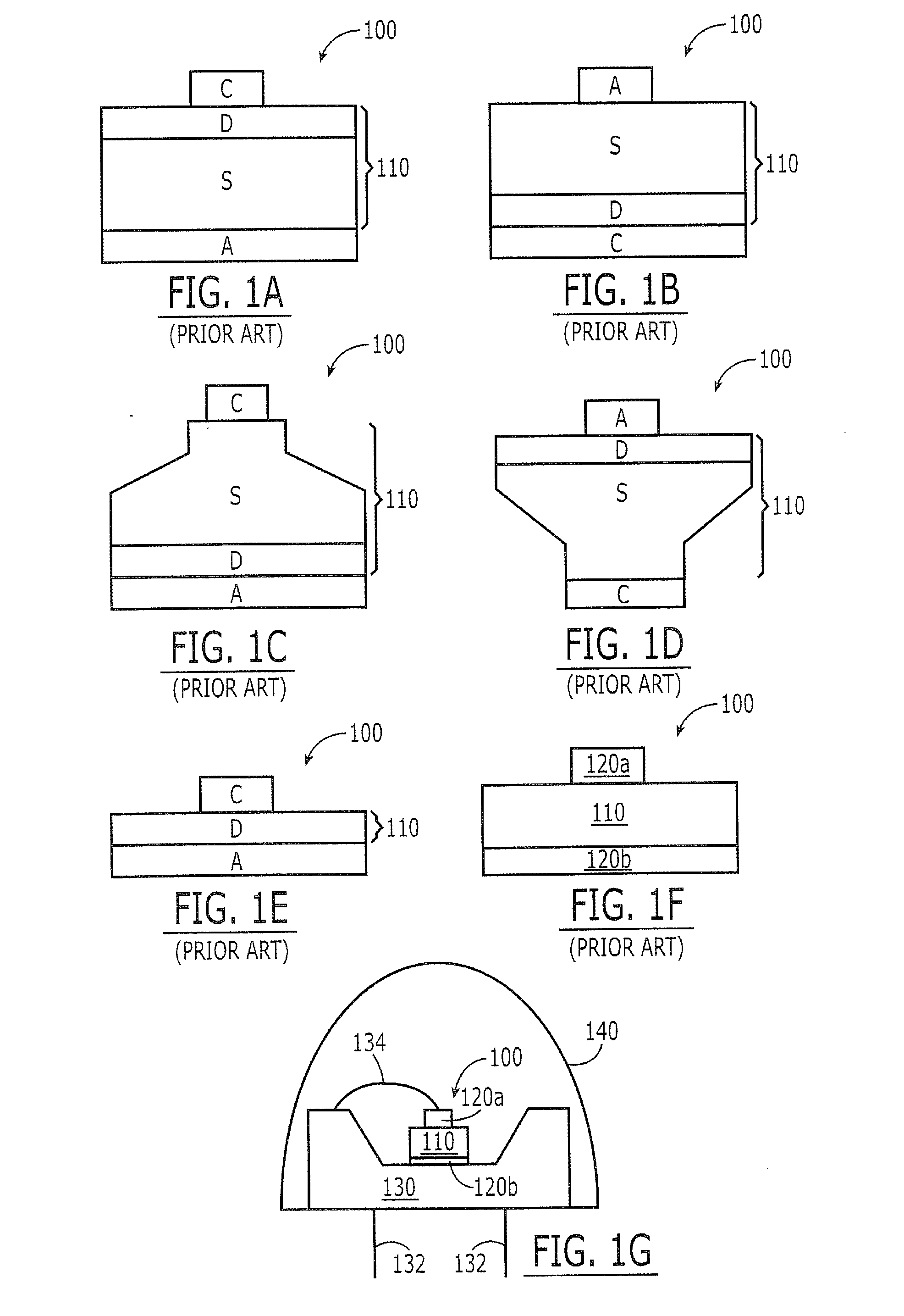
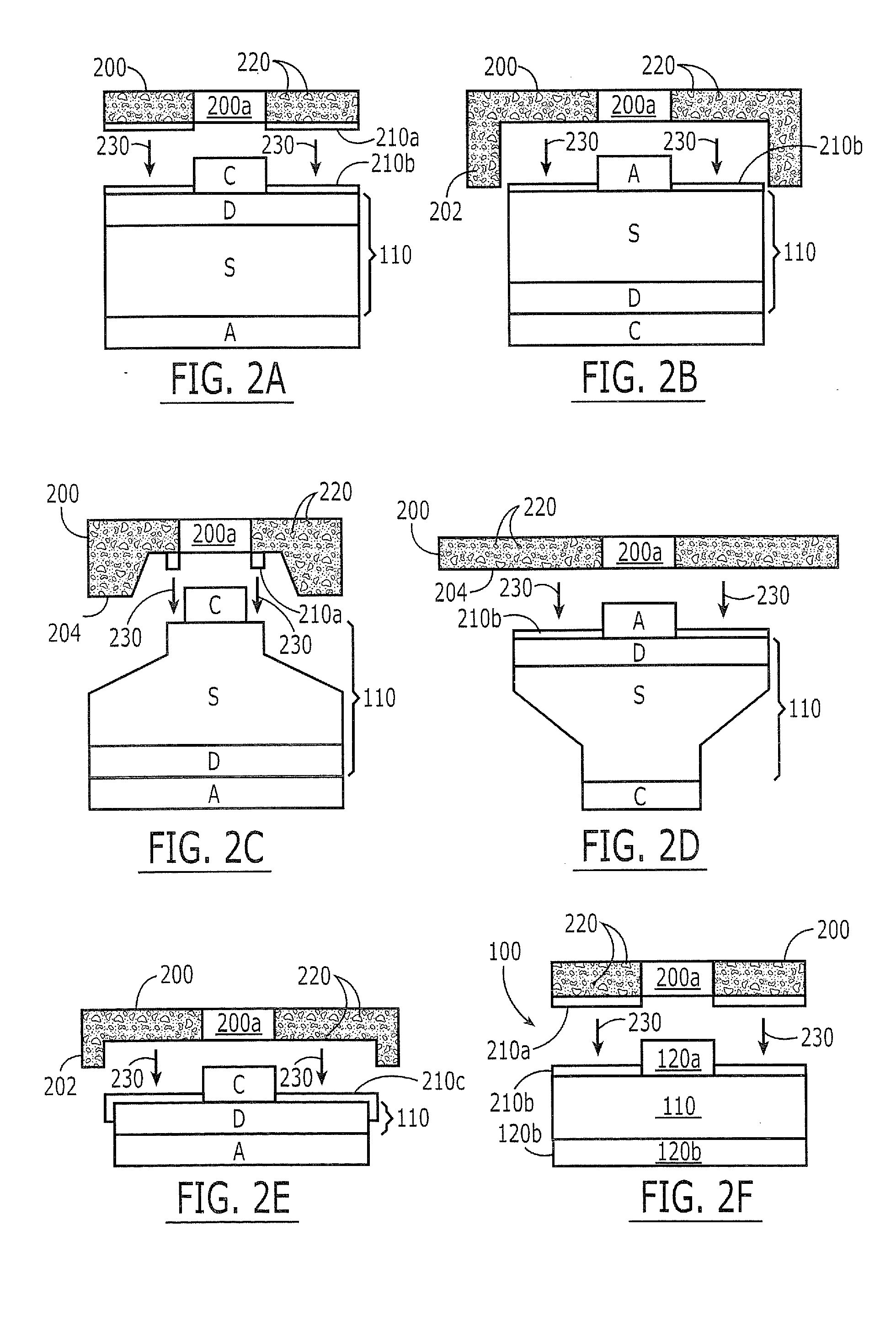
[0039]The invention will be described more fully hereinafter with reference to the accompanying drawings, in which example embodiments of the invention are shown. This invention may, however, be embodied in many different forms and should not be construed as limited to the example embodiments set forth herein. Rather, the disclosed embodiments are provided so that this disclosure will be thorough and complete, and will fully convey the scope of the invention to those skilled in the art. In the drawings, the size and relative sizes of layers and regions may be exaggerated for clarity. Moreover, each embodiment described and illustrated herein includes its complementary conductivity type embodiment as well. Like numbers refer to like elements throughout.

[0040]It will be understood that when an element or layer is referred to as being “connected to,”“coupled to” or “responsive to” (and / or variants thereof) another element, it can be directly connected, coupled or responsive to the othe...


PUM


Abstract

A preform is attached to a solid state light emitting die. One or more optical elements, such as a photoluminescent element, a refracting element, a filtering element, a scattering element, a diffusing element or a reflecting element, is included in and/or on the preform. For example, the preform may be a glass preform with phosphor particles suspended therein. The preform may be fabricated using microelectronic manufacturing techniques, and may be placed on the solid state light emitting die using pick and place techniques.

Description

FIELD OF THE INVENTION[0001]This invention relates to solid state light emitting devices and fabrication methods therefor, and more particularly to packaging for solid state light emitting dice.BACKGROUND OF THE INVENTION[0002]Solid state light emitting devices, such as inorganic or organic Light Emitting Diodes (LEDs), are widely used for many applications. As is well known to those having skill in the art, a solid state light emitting device includes a solid state light emitting die or chip that is configured to emit coherent and / or incoherent light upon energization thereof. An inorganic LED may include semiconductor layers that form P-N junctions. An organic LED may include one or more organic light emission layers. Typically, a solid state light emitting device generates light through the recombination of electronic carriers, i.e., electrons and holes, in a light emitting layer or region.[0003]It is also known that a solid state light emitting die may be packaged to provide ext...

Claims


Application Information

Patent Timeline
Patent Type & Authority Applications(United States)
IPC IPC(8): H01L33/00H01L33/50H01L33/58
CPCH01L33/505H01L33/58H01L2933/0091H01L2224/48091H01L2224/73265H01L2924/00014
Inventor ANDREWS, PETER S.TOQUIN, RONAN P. LE
Owner CREE INC
Why Eureka
Try Eureka