Organic electroluminescent display device and method of fabricating the same

Active Publication Date: 2008-05-29
LG DISPLAY CO LTD
View PDF3 Cites 10 Cited by
  • Summary
  • Abstract
  • Description
  • Claims
  • Application Information

AI Technical Summary

Benefits of technology

[0030]An advantage of the present invention is to provide an OELD device with a uniform luminance and prevent decreasing of lifetime of the OELD device.
[0031]Additional features and advantages of the invention will be set forth in the description which follows, and in part will be apparent from the description, or may be learned by practice of the invention. These and other advantages of the invention will be realized and attained by the structure particularly pointed out in the written description and claims hereof as well as the appended drawings.
[0032]To achieve these and other advantages and in accordance with the purpose of the present invention, as embodied and broadly described herein, an organic electroluminescent display (OELD) device includes first and second substrates facing each other; a plurality of gate lines, a plurality of data lines and a plurality of power lines on the first substrate, the gate and data lines crossing each other to define a plurality of pixel regions, a switching element and a driving element connected to each other in each pixel region, a first electrode connected to the driving element, an organic luminescent layer on the first electrode, and a second electrode on the organic luminescent layer. The organic luminescent layer includes a hole injection layer, a hole transporting layer, an emission material layer, an electron transporting layer, and an electron injection layer in order. Further, the hole injection layer includes a crystallizable hole injection material and a hole transporting material, and the hole transporting layer includes the hole transporting material.
[0033]In another aspect of the present invention, a method of fabricating an organic electroluminescent diode for an organic electroluminescent display (OELD) device includes forming

Problems solved by technology

Moreover, due to their simple fabricating process, the fabrication costs of OELD devices are low when compared with those of LCD devices.
However, the passive matrix type OELD devices have disadvantages of high power consumption and low quality images.
However, the crystallizable material has an un-uniform arrangement of grains.
It causes deterioration in the organic elec

Method used


Image

  • Organic electroluminescent display device and method of fabricating the same
  • Organic electroluminescent display device and method of fabricating the same
  • Organic electroluminescent display device and method of fabricating the same

Examples


Embodiment Construction

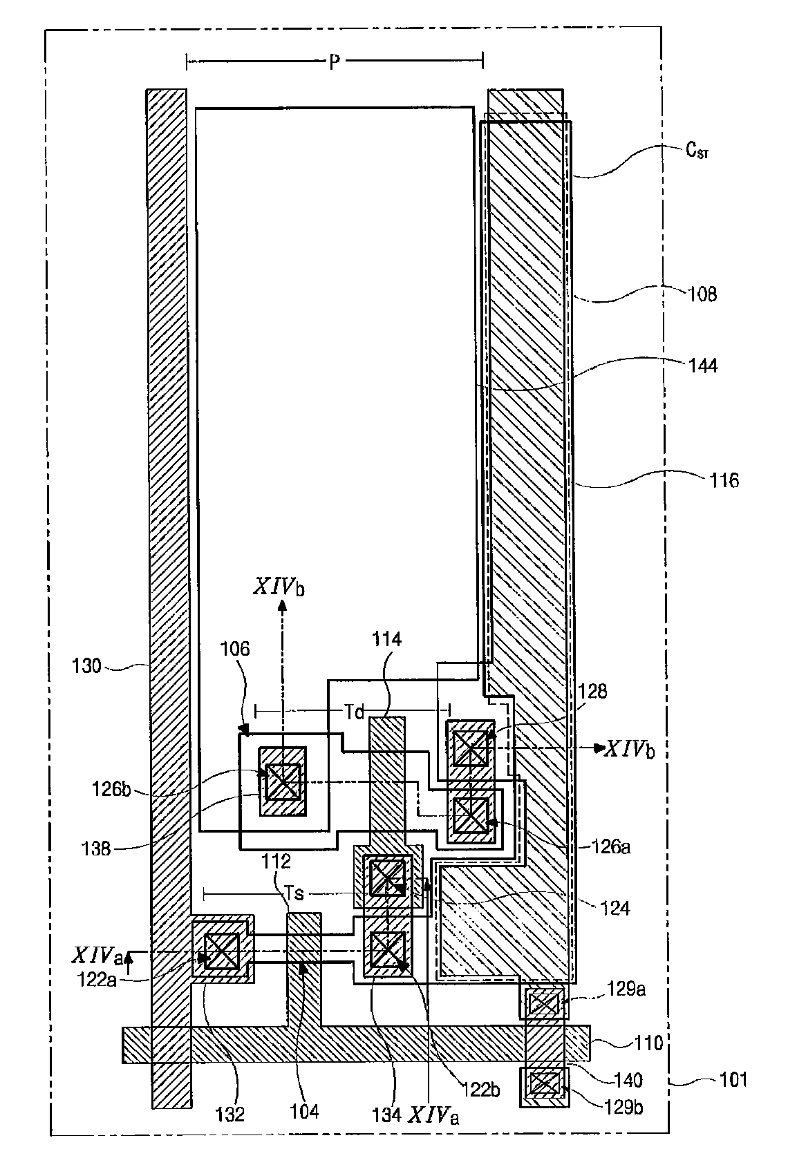
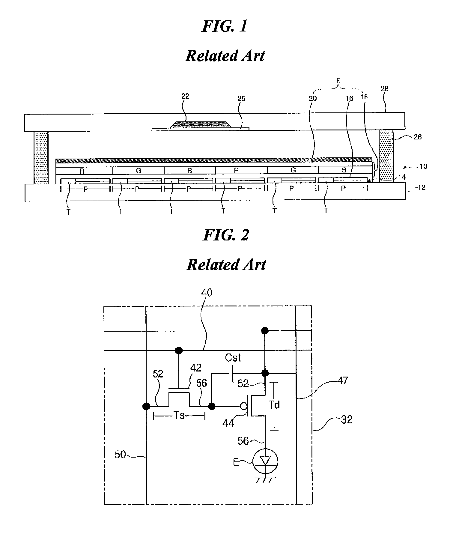
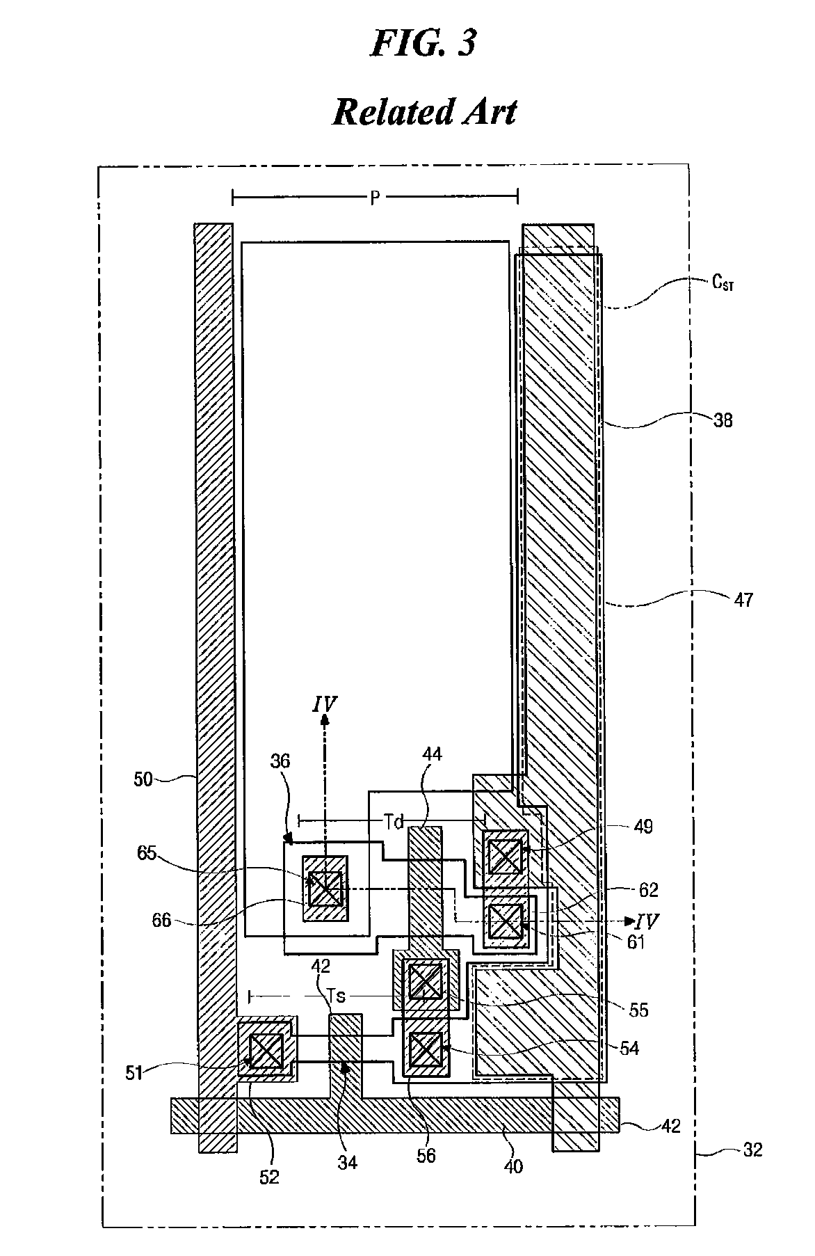
[0053]Reference will now be made in detail to embodiments of the present invention, examples of which are illustrated in the accompanying drawings. The same reference numbers may be used throughout the drawings to refer to the same or like parts.

[0054]As the present invention may be embodied in several forms without departing from the spirit or essential characteristics thereof, it should also be understood that the above-described embodiments are not limited by any of the details of the foregoing description, unless otherwise specified, but rather should be construed broadly within its spirit and scope as defined in the appended claims, and therefore all changes and modifications that fall within the metes and bounds of the claims, or equivalence of such metes and bounds are therefore intended to be embraced by the appended claims.

[0055]In an OELD device of the present invention, a hole injection layer includes a first material forming the hole injection layer in a conventional OEL...


PUM


Abstract

An organic electroluminescent display (OELD) device includes first and second substrates facing each other, a plurality of gate lines, a plurality of data lines and a plurality of power lines on the first substrate, the gate and data lines crossing each other to define a plurality of pixel regions, a switching element and a driving element connected to each other in each pixel region, a first electrode connected to the driving element, an organic luminescent layer on the first electrode, and a second electrode on the organic luminescent layer. The organic luminescent layer includes a hole injection layer, a hole transporting layer, an emission material layer, an electron transporting layer, and an electron injection layer in order. Further, the hole injection layer includes a crystallizable hole injection material and a hole transporting material, and the hole transporting layer includes the hole transporting material.

Description

[0001]The present application claims the benefit of Korean Patent Application No. 2006-0118600 filed in Korea on Nov. 28, 2006, which is hereby incorporated by reference for all purposes as if fully set forth herein.BACKGROUND OF THE INVENTION[0002]1. Field of the Invention[0003]The present invention relates to an organic electroluminescent display (OELD) device, and more particularly, to an OELD device including a hole injection layer having an improved properties and method for fabricating the same.[0004]2. Discussion of the Related Art[0005]In general, organic electroluminescent display (OELD) devices emit light by injecting electrons from a cathode and holes from an anode into an emission material layer, combining the electrons with the holes, generating excitons, and transforming the excitons of an excited state to a ground state. Unlike liquid crystal display (LCD) devices, OELD devices do not require an additional light source and therefore have the advantages of slimness and...

Claims


Application Information

Patent Timeline
IPC IPC(8): H01L51/54H01L51/56
CPCH01L27/3244H01L51/5088H01L51/5048H10K59/12H10K50/14H10K50/17C09K11/06Y02B20/30Y10S428/917
Inventor KIM, YOUNG-MILIM, HYUN-TAEKPARK, JONG-HYUN
Owner LG DISPLAY CO LTD
Why Eureka
Try Eureka