Thin film transistor liquid crystal display
a thin film transistor and liquid crystal display technology, applied in non-linear optics, instruments, optics, etc., can solve the problems of poor performance, light leakage, and difficult post-separation return, and achieve the effect of stable configuration
- Summary
- Abstract
- Description
- Claims
- Application Information
AI Technical Summary
Benefits of technology
Problems solved by technology
Method used
Image

Examples
first embodiment
The First Embodiment
[0048]The TFT LCD according to the first embodiment of the present invention comprises a color filter substrate, a TFT array substrate, a liquid crystal layer sealed between the color filter substrate and the TFT array substrate, and post spacers are disposed between the color filter substrate and the TFT array substrate to maintain the cell gap between the substrates after assembling.
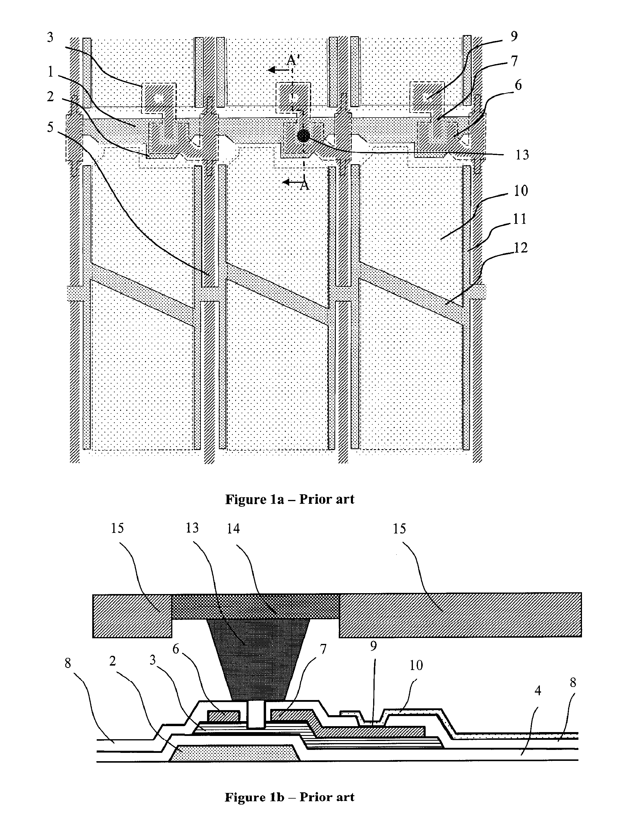
[0049]FIG. 3a is a schematic plan view showing the TFT LCD according to the first embodiment of the present invention. As shown in FIG. 3a, there are a plurality of gate lines 1, a plurality of common electrodes 12, and a plurality of data lines 5 perpendicular to the gate lines 1 arranged on the TFT array substrate of the TFT LCD. The adjacent gate lines and data lines cross with each other to define pixel areas. Each pixel area comprises a TFT switching device, a transparent pixel electrode 10, a light blocking bar 11, and a part of the common electrode 12. As shown in FIGS. 3a an...
second embodiment
The Second Embodiment
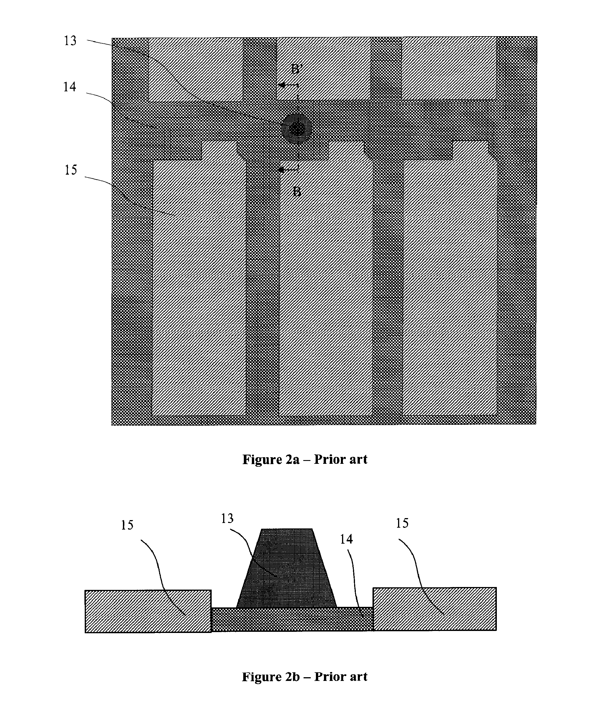
[0061]In the first embodiment, the post spacer contacts the pixel electrode formed on the passivation layer, as shown in FIGS. 3b and 3c, while in a second embodiment, the post spacer contacts the pixel electrode formed directly on the glass substrate as the underlying substrate with the passivation layer and the gate insulating layer being removed by an opening etching method, as shown in FIGS. 6a and 6b. The sidewall of the opening 16 has a sloping angle in a range of about 20-90 degree.
[0062]The step difference around the post spacer 13 is increased with such design so as to limit the movement of the post spacer more effectively. In order to maintain the same cell gap as that in the first embodiment after assembling, it is necessary to further increase the height of the post spacer 13 by an increment that is equal to the sum of the passivation layer 8 and the gate insulating layer 4. Optionally, the depth of the opening can be also smaller than the sum of the...
third embodiment
The Third Embodiment
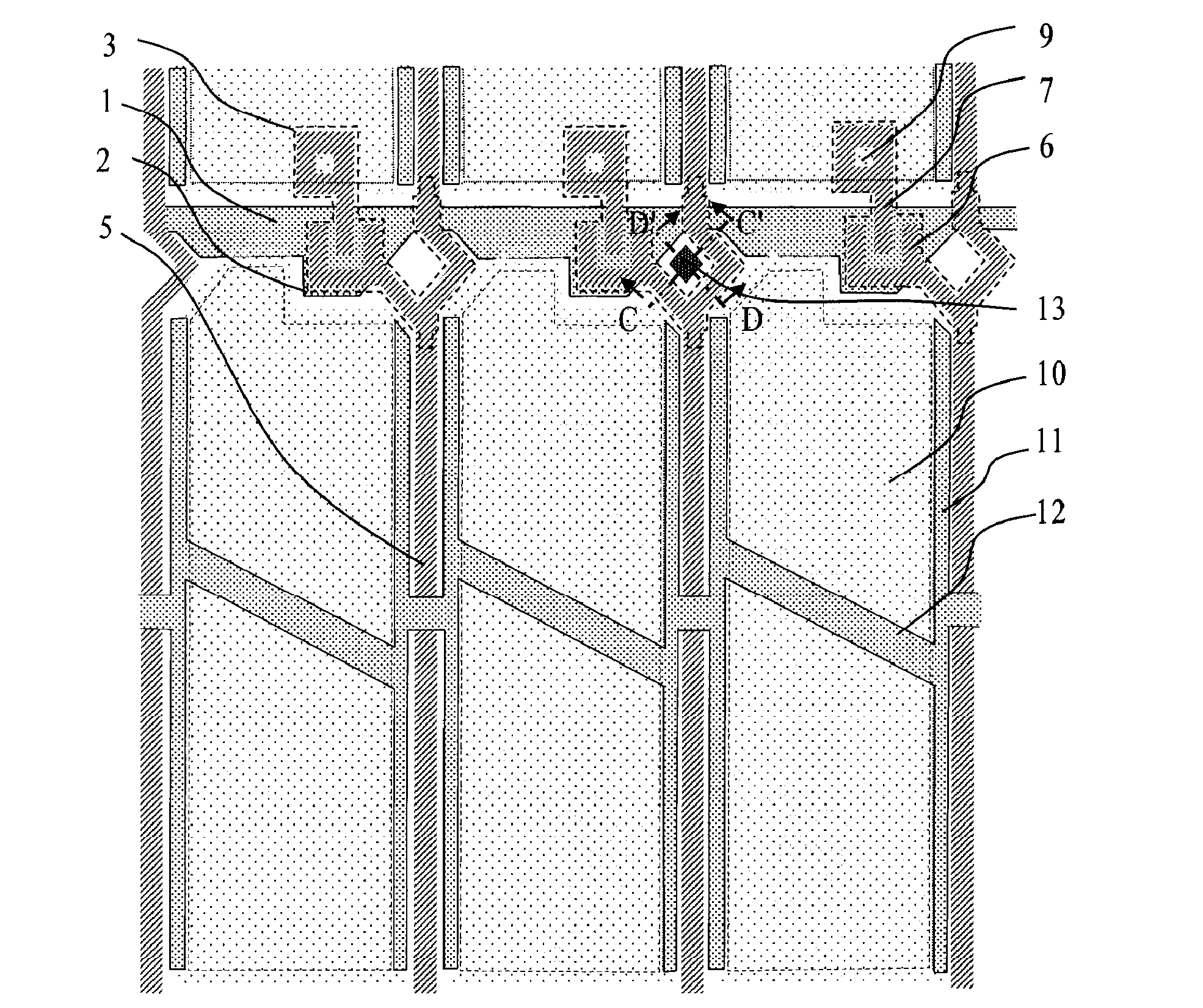
[0066]FIG. 9a is a schematic plan view showing the TFT LCD according to a third embodiment of the present invention. As shown in FIG. 9a, there are a plurality of gate lines 1, a plurality of common electrodes 12, and a plurality of data lines 5 perpendicular to the gate lines 1 arranged on the TFT array substrate of the TFT LCD. The adjacent gate lines and data lines cross with each other to define pixel areas. Each pixel area comprises a TFT switching device, a transparent pixel electrode 10, a light blocking bar 11, and a part of the common electrode 12. As shown in FIGS. 9a and 9c, each of the TFT devices comprises a gate electrode 2, a gate insulating layer 4, a semiconductor active layer 3, and a source electrode 6 and a drain electrode 7. A transparent pixel electrode 10 is connected to the drain electrode 7 of the TFT via a through-hole 9 in a passivation layer 8.
[0067]According to the third embodiment of the present invention, the shape of a part of the ...
PUM
 Abstract
Description
Claims
Application Information
 - R&D
- Intellectual Property
- Life Sciences
- Materials
- Tech Scout
- Unparalleled Data Quality
- Higher Quality Content
- 60% Fewer Hallucinations
Browse by: Latest US Patents, China's latest patents, Technical Efficacy Thesaurus, Application Domain, Technology Topic, Popular Technical Reports.
© 2025 PatSnap. All rights reserved.Legal|Privacy policy|Modern Slavery Act Transparency Statement|Sitemap|About US| Contact US: help@patsnap.com