Electrostatic discharge protection circuit using triple welled silicon controlled rectifier

a protection circuit and silicon control technology, applied in semiconductor devices, semiconductor/solid-state device details, diodes, etc., can solve the problems of circuit degrading driving capability, circuit damage caused by esd phenomenon, and adverse effects on the ic of the semiconductor, etc., to achieve great discharge capacity

Active Publication Date: 2008-06-05
ELECTRONICS & TELECOMM RES INST
View PDF12 Cites 6 Cited by
  • Summary
  • Abstract
  • Description
  • Claims
  • Application Information

AI Technical Summary

Benefits of technology

[0019]In addition, the present invention provides an ESD protection circuit using an SCR, which requires a low trigger voltage and has great discharge capacity.

Problems solved by technology

When a high voltage is applied to a semiconductor integrated circuit (IC) due to the ESD phenomenon, the semiconductor IC may be adversely affected or incapable of functions.
Therefore, it is probable that damage caused by the ESD phenomenon will become greater.
However, because the ESD protection circuit has insufficient current discharge capacity, its size should be enlarged to obtain a reliable ESD protection effect.
Therefore, the ESD protection circuit degrades driving capability and cannot be highly integrated.
However, since a trigger (driving) voltage of the SCR is as high as about 20 to 30 V, when it is applied to a metal oxide semiconductor field effect transistor (MOSFET) that is fabricated on the DSM scale, it is difficult to effectively remove an ESD pulse before a gate oxide layer is broken.

Method used


Image

  • Electrostatic discharge protection circuit using triple welled silicon controlled rectifier
  • Electrostatic discharge protection circuit using triple welled silicon controlled rectifier
  • Electrostatic discharge protection circuit using triple welled silicon controlled rectifier

Examples


Embodiment Construction

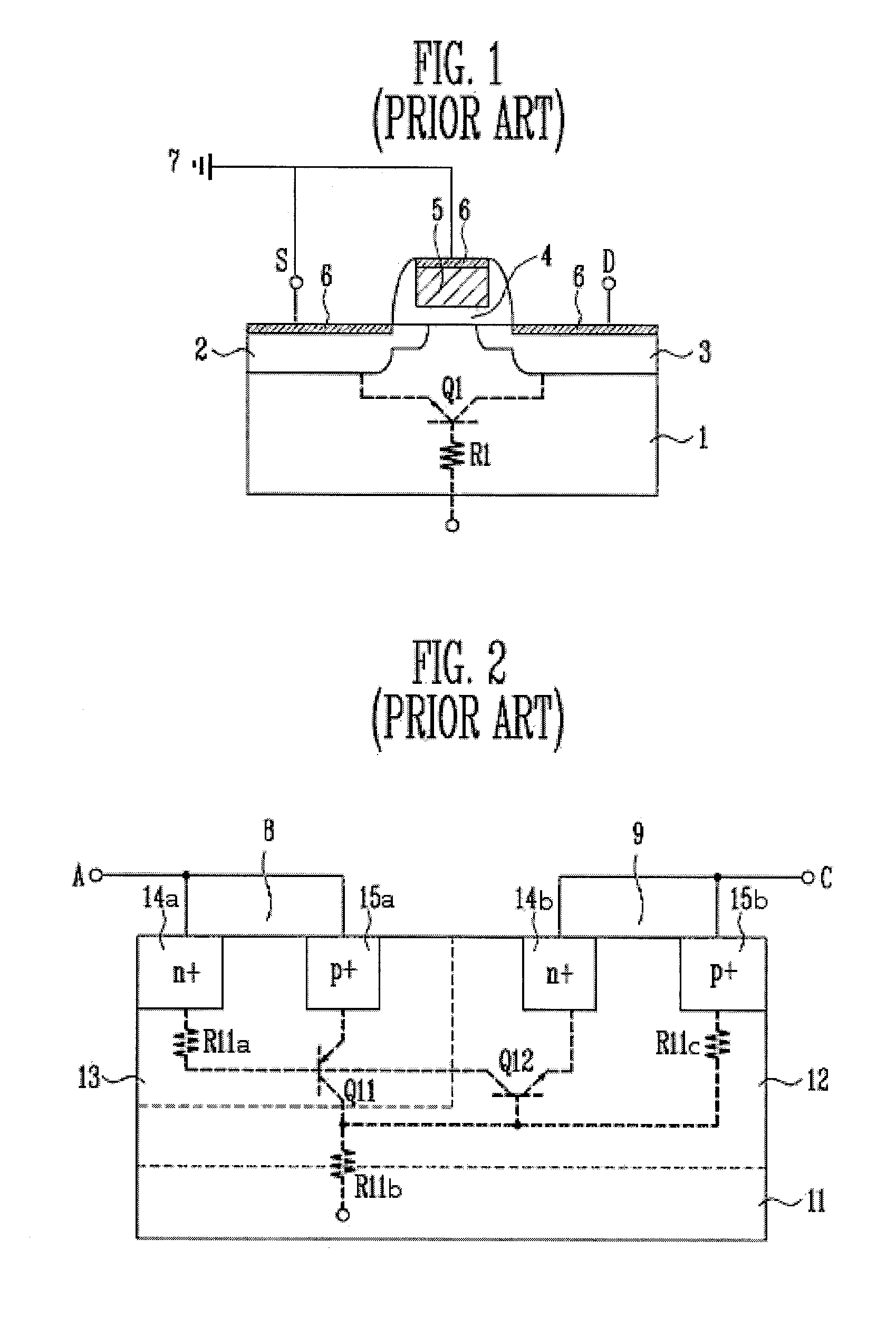
[0030]The present invention will now be described more fully hereinafter with reference to the accompanying drawings, in which exemplary embodiments of the invention are shown. This invention may, however, be embodied in different forms and should not be construed as limited to the embodiments set forth herein. Rather, these embodiments are provided so that this disclosure is thorough and complete and fully conveys the scope of the invention to those skilled in the art.

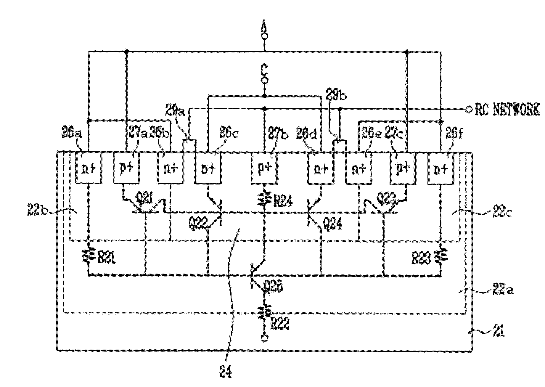
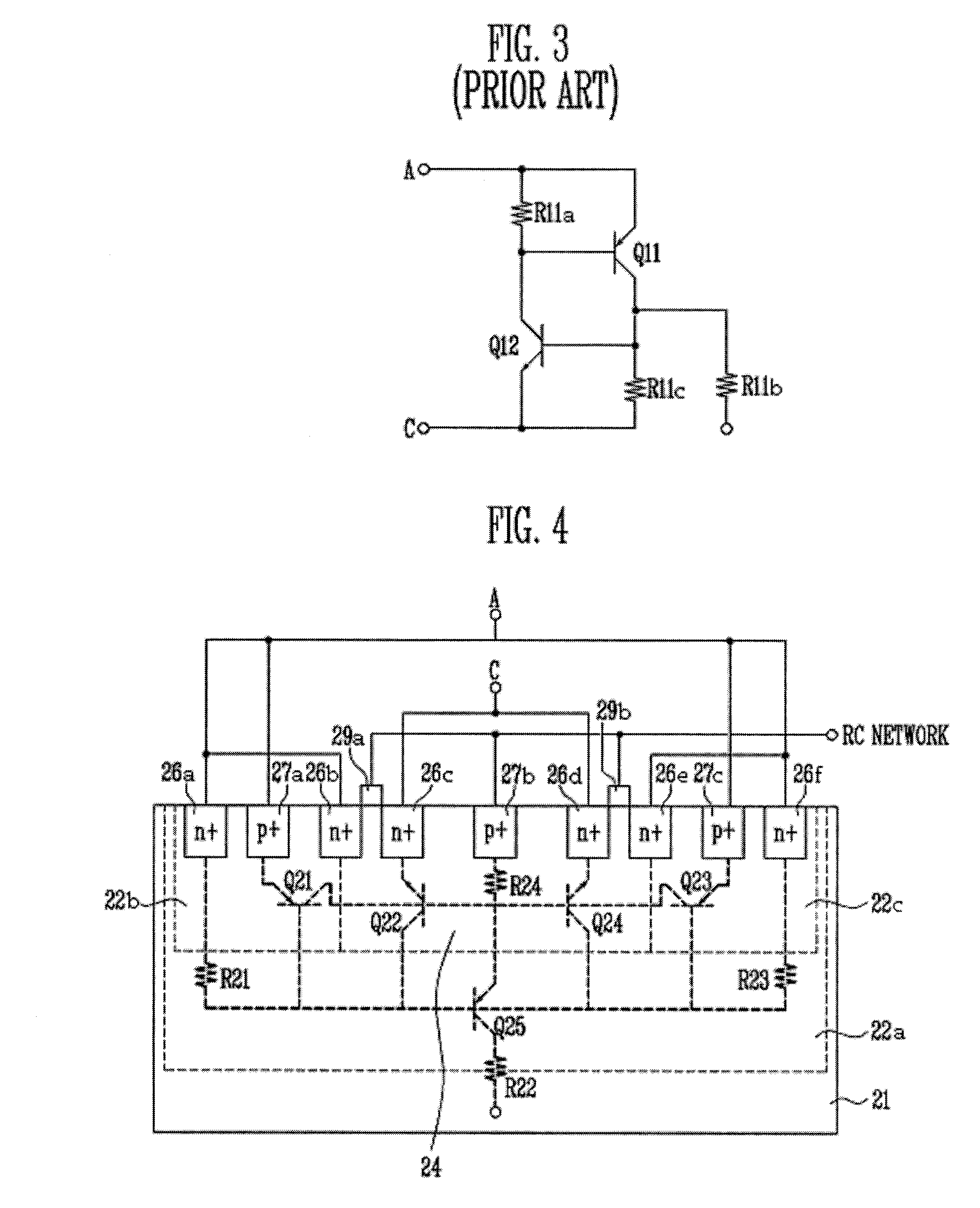
[0031]FIG. 4 is a cross-sectional view of an electrostatic discharge (ESD) protection circuit using a silicon controlled rectifier (SCR) according to an exemplary embodiment of the present invention.

[0032]The ESD protection circuit according to the present invention is formed in a p-type semiconductor substrate 21 having a triple well structure. The p-type semiconductor substrate 21 having the triple well structure includes an n-well 22a and an n-well 22b, a p-well 24, and an n-well 22c, which are formed in the n-well...


PUM


Abstract

Provided is an electrostatic discharge (ESD) protection circuit using a silicon controlled rectifier (SCR), which is applied to a semiconductor integrated circuit (IC). A semiconductor substrate has a triple well structure such that a bias is applied to a p-well corresponding to a substrate of a ggNMOS device. Thus, a trigger voltage of the SCR is reduced. In addition, two discharge paths are formed using two SCRs including PNP and NPN bipolar transistors. As a result, the ESD protection circuit can have greater discharge capacity.

Description

CROSS-REFERENCE TO RELATED APPLICATION[0001]This application claims priority to and the benefit of Korean Patent Application No. 2004-105736, filed Dec. 14, 2004 and Korean Patent Application No. 2005-37956, filed May 6, 2005, the disclosure of which is incorporated herein by reference in its entirety.BACKGROUND[0002]1. Field of the Invention[0003]The present invention relates to an electrostatic discharge (ESD) protection circuit for a low-voltage circuit, which is applied to a semiconductor integrated circuit (IC), and more specifically, to an ESD protection circuit using a silicon controlled rectifier (SCR).[0004]2. Discussion of Related Art[0005]An electrostatic discharge (ESD) phenomenon, which causes the instantaneous application of a high voltage due to static electricity that is induced by contact with a human body, frequently occurs during the fabrication or use of semiconductor components or electronic products. When a high voltage is applied to a semiconductor integrated ...

Claims


Application Information

Patent Timeline
Patent Type & Authority Applications(United States)
IPC IPC(8): H01L23/62
CPCH01L29/7436H01L29/749H01L29/87H01L2924/0002H01L2924/00
Inventor KIM, KWI DONGKWON, CHONG KIKIM, JONG DAE
Owner ELECTRONICS & TELECOMM RES INST
Why Eureka
Try Eureka