Liquid crystal display device, manufacturing method of liquid crystal display device and mother substrate of liquid crystal display device

Inactive Publication Date: 2008-06-12
HITACHI DISPLAYS
View PDF4 Cites 15 Cited by
  • Summary
  • Abstract
  • Description
  • Claims
  • Application Information

AI Technical Summary

Benefits of technology

[0022]According to means (7), since the end sealing material for sealing the sealing inlet contacts the edge sealing material, it is possible to improve a reliability of a end sealing portion.
[0023]According to means (8), (9), and (10), since the columnar member is formed in the vicinity of the sealing inlet in advance when applying the edge sealing material so as to have the sealing inlet on the second substrate and the edge sealing material is prevented from running over to the adjacent liquid crystal cells by allowing the edge sealing material to contact the columnar member when superimposing the second substrate on the first substrate, it is possible to improve an a degree of accuracy of the edge sealing portion.
[0024]According to means (11) and (12), since the edge sealing material can be prevented from running over f

Problems solved by technology

In “Patent Document 1” described above, the technique in which edge sealing material is coated accurately by computer control is disclosed, however, there remains the problem that the distance between adjacent liquid crystal cells is small in the vicinity of the liquid crystal sealing inlet in which the interference of edge sealing material is particularly controversial, and the edge sealing material protrudes to cause interference with adjacent cells.
Therefore, in order to avoid the problem that the edge sealing material runs ov

Method used


Image

  • Liquid crystal display device, manufacturing method of liquid crystal display device and mother substrate of liquid crystal display device
  • Liquid crystal display device, manufacturing method of liquid crystal display device and mother substrate of liquid crystal display device
  • Liquid crystal display device, manufacturing method of liquid crystal display device and mother substrate of liquid crystal display device

Examples


embodiment 1

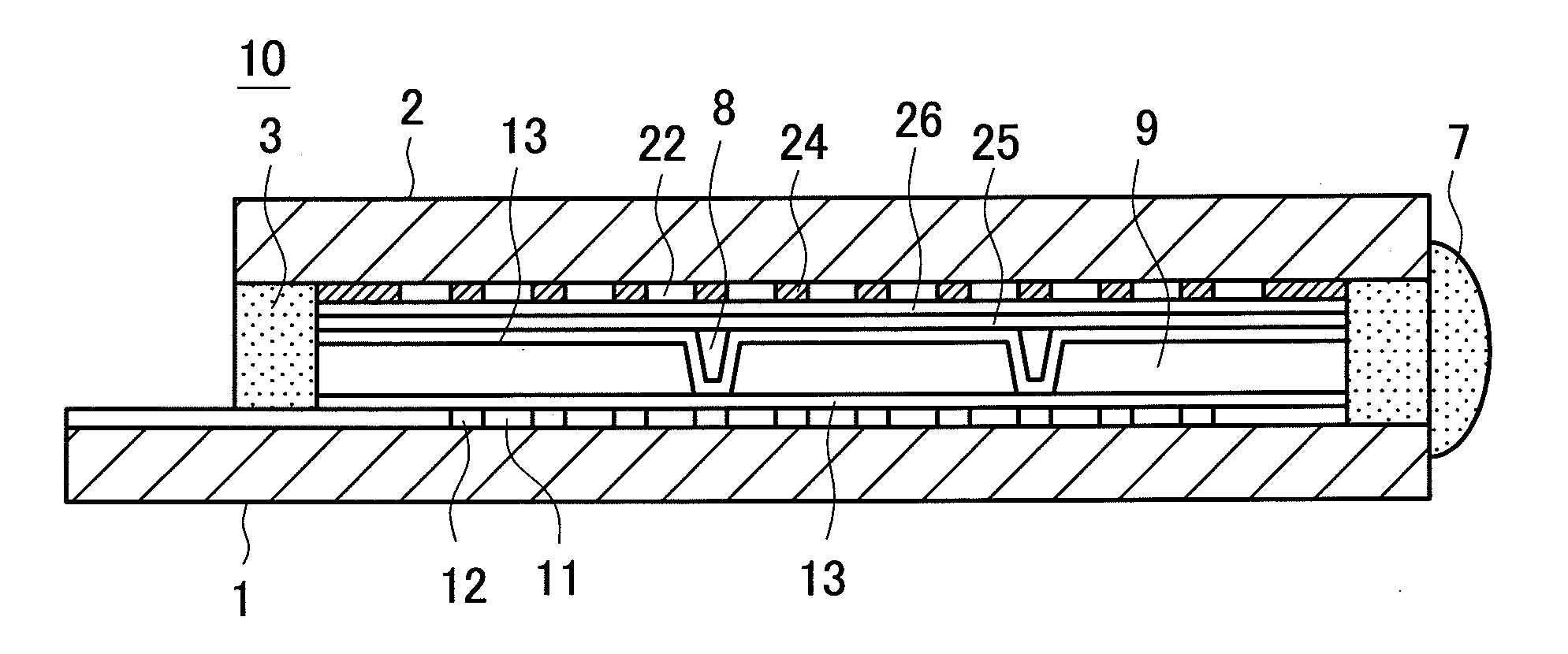
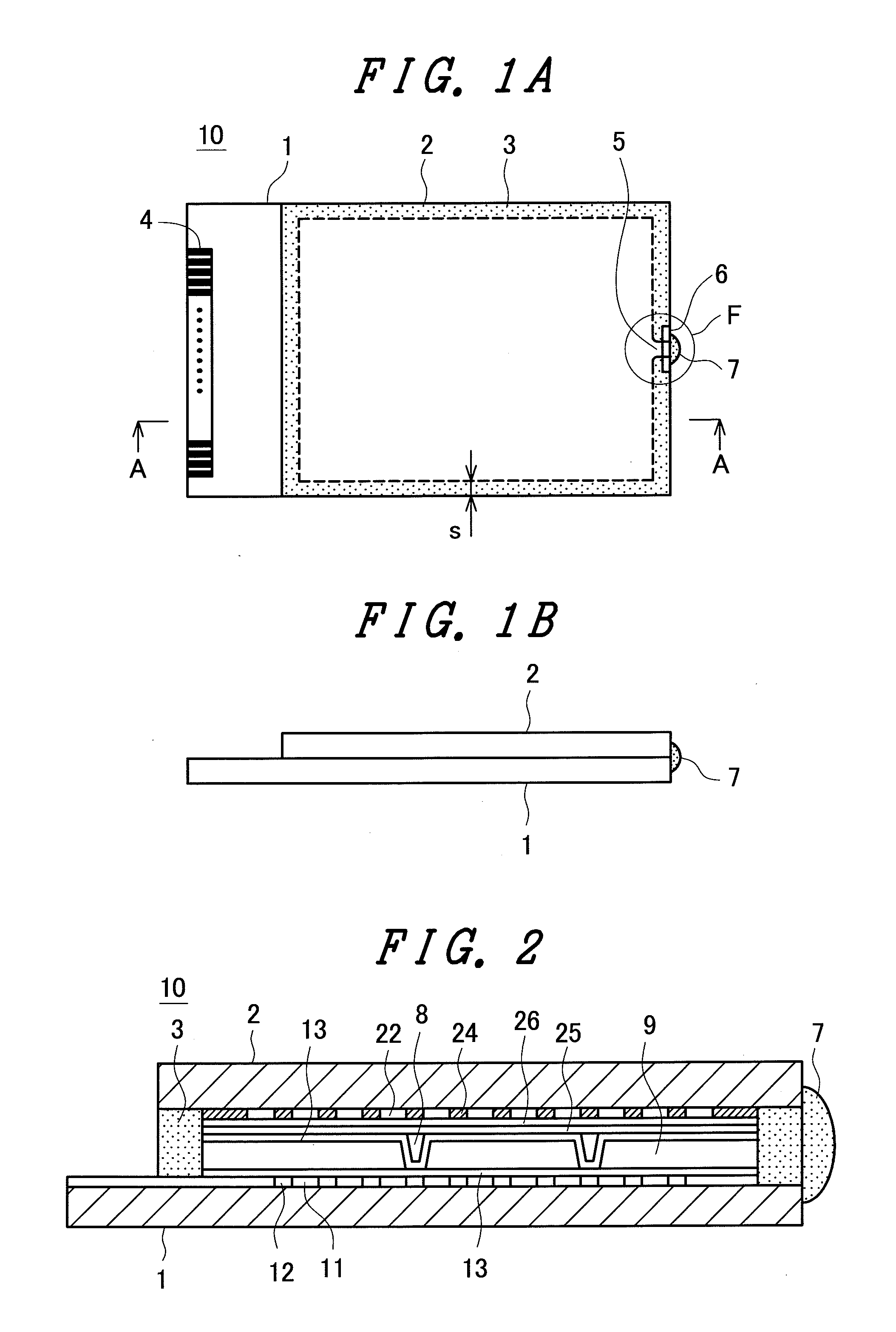
[0046]FIG. 1A and FIG. 1B are outline views showing a liquid crystal cell 10 according to a first embodiment of the invention, in which FIG. 1A is a plan view and FIG. 1B is a side view. In FIG. 1A, on a TFT substrate 1 in which pixel electrodes 11, TFT 12 and the like are formed in a matrix state, an opposite substrate 2 in which color filters and the like are formed is stacked and bonded through a edge sealing material 3. The color filters may be attached to the TFT substrate. The edge sealing material 3 is made of organic resin, and a width “s” of the edge sealing material 3 is approximately 0.7 mm. A gap of several μm is formed between the TFT substrate 1 and the opposite substrate 2, and a liquid crystal 9 is filled there between. On the TFT substrate 1, a terminal portion 4, not-shown driving IC chips and the like are attached, therefore, the TFT substrate is formed larger than the opposite substrate 2. A flexible wiring board is attached to the terminal portion 4 for supplyin...

embodiment 2

[0074]FIG. 18 shows a second embodiment according to the present invention. The liquid crystal cell 10 is required to make the plate thickness of the TFT substrate 1 or the opposite substrate 2 smaller for making the thickness of the entire display device smaller. The TFT substrate 1 or the opposite substrate 2 is made of a glass. The thickness of a glass substrate is standardized and generally, the thickness is about 0.5 mm. If the thickness of the glass substrate is changed, the cost of the glass substrate is increased. In addition, the manufacturing device also adapts to the standardized thickness of the glass substrate, so that it is difficult to manufacture the display device if the glass substrate of thinner plate thickness is used.

[0075]However, the side of the display device may demand the TFT substrate 1 or the opposite substrate 2 with the plate thickness of about 0.2 mm. As means for responding to this demand, there is a method to make the glass substrate thinner by polis...


PUM


Abstract

A liquid crystal sealing inlet is formed by a edge sealing material, and a sealing-inlet columnar spacer is formed so as to prevent the edge sealing material from running over to adjacent liquid crystal cells when bonding a TFT substrate and a color filter substrate together.

Description

[0001]The present application claims priority from Japanese applications JP2006-331433 filed on Dec. 8, 2006, the content of which is hereby incorporated by reference into this application.BACKGROUND OF THE INVENTION[0002]The invention relates to a liquid crystal display device, particularly, relates to a configuration in which many liquid crystal cells can be obtained from a mother substrate.[0003]In the liquid crystal display device, in a general way, many liquid-crystal cell substrates are formed on a large grass substrate (mother substrate) according to the request on manufacturing costs, and manufacturing processes are performed in the unit of the mother substrate, then, after the completion, liquid crystal cells are cut off.[0004]A liquid crystal cell is formed by a TFT substrate in which pixel electrodes, thin-film transistors (TFTs) and the like are formed and an opposite substrate in which color filters and the like are formed. Many TFT substrates are formed at a time by be...

Claims


Application Information

Patent Timeline
IPC IPC(8): G02F1/1339H01J9/26
CPCG02F1/133351G02F1/1341G02F1/13394
Inventor NAGAMI, TAKAHIROENDO, HIROAKI
Owner HITACHI DISPLAYS
Why Eureka
Try Eureka