Chip component

a chip and component technology, applied in the manufacture of resistor chips, waveguide devices, fixed capacitor details, etc., can solve the problems of deformation of circuit patterns from substrates, deformation of electrical characteristics of chip components, and deformation of circuit patterns, so as to reduce the number of occurrences of deformation and partial detachment

US20080142251A1Inactive Publication Date: 2008-06-19MURATA MFG CO LTD
11 Cites 1 Cited by

Patent Information

Authority / Receiving Office
US · United States
Current Assignee / Owner
Publication Date
2008-06-19
Estimated Expiration
Not applicable · inactive patent

Smart Images

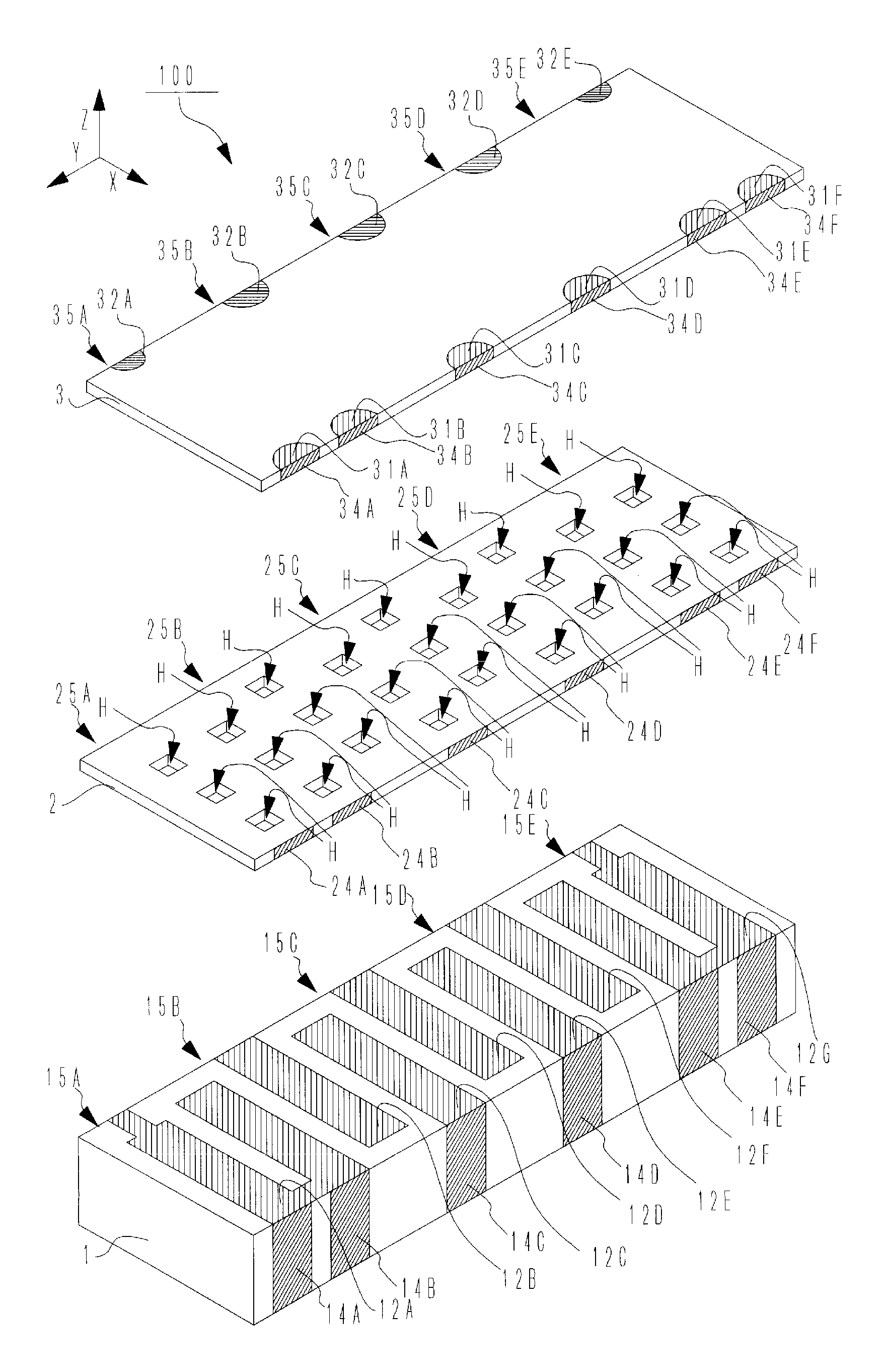
  • Figure 1
    Figure 1
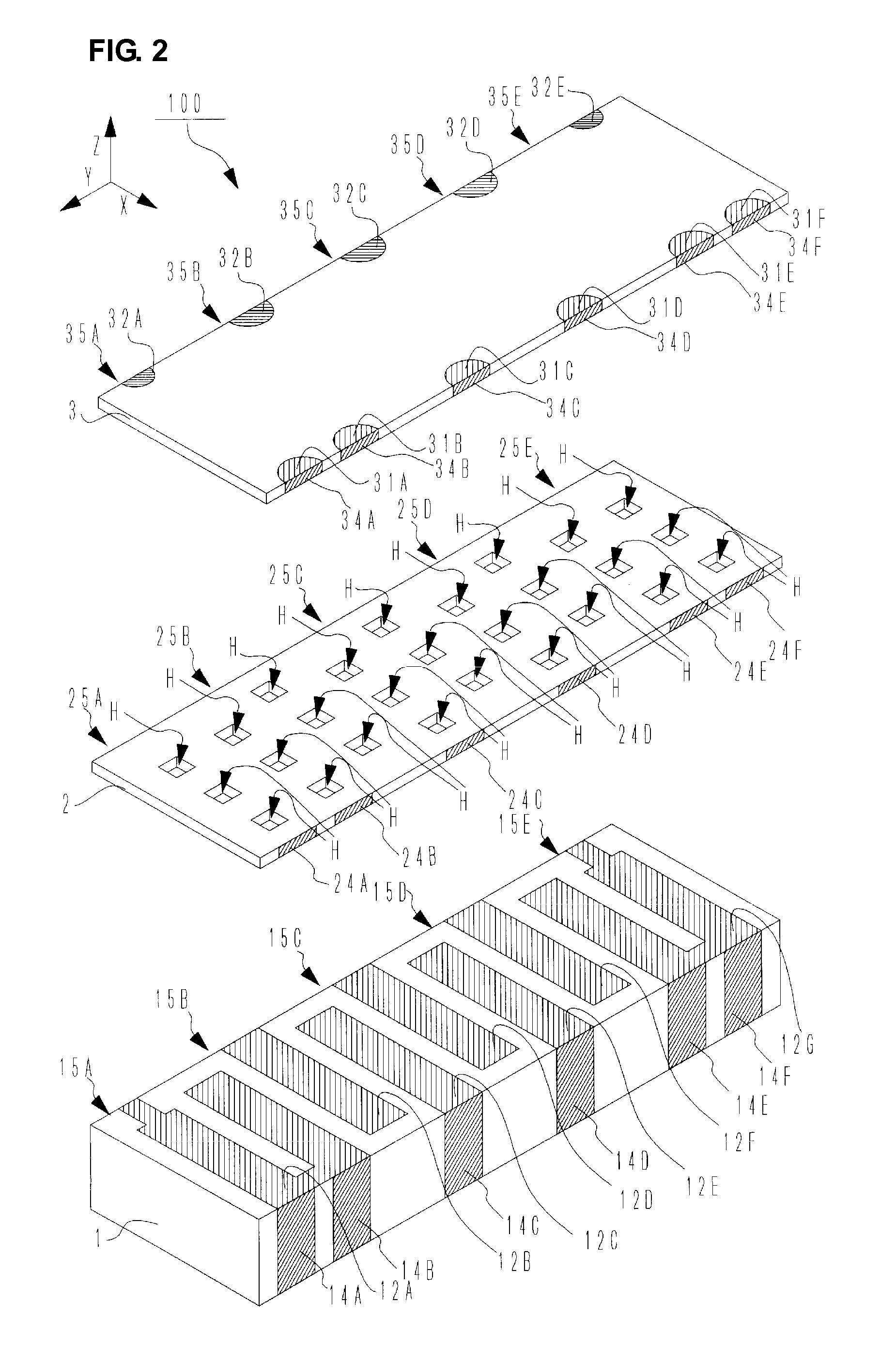
  • Figure 2
    Figure 2
  • Figure 3
    Figure 3
Patent Text Reader

Abstract

A chip component is obtained by laminating a dielectric substrate, a first insulating layer provided on a principal surface of the dielectric substrate, and a second insulating layer covering substantially the entire first insulating layer. A circuit pattern includes a resonance line provided in an interface between the dielectric substrate and the first insulating layer. A plurality of through holes (H) are aligned n the first insulating layer along an extending direction of the circuit pattern at locations facing an area within the boundary of the circuit pattern.
Need to check novelty before this filing date? Find Prior Art

Description

BACKGROUND OF THE INVENTION

[0001] 1. Field of the Invention

[0002] The present invention relates to chip components having a circuit pattern on a dielectric substrate.

[0003] 2. Description of the Related Art

[0004] A photolithographic is known for producing chip components. In the method, extremely accurate circuit patterns are formed by printing, exposing, and developing a photosensitive conductive paste on a dielectric substrate (See Japanese Unexamined Patent Application Publication No. 2001-210541).

[0005] Such a chip component provided with a circuit pattern formed using the photolithographic method has a low adhesion strength for the circuit pattern over the dielectric substrate. This may result in the circuit pattern becoming detached from the substrate due to thermal factors or mechanical factors. Once such detachment occurs in the circuit pattern, the conductivity of the circuit pattern is degraded, which degrades the reliability of the chip component.

[0006] To avoid such circuit pa...

Examples

Embodiment Construction

[0031]A chip component according to preferred embodiments of the present invention is described with reference to drawings. The Cartesian coordinate system (X-Y-Z axes) shown in the drawings is used for the description.

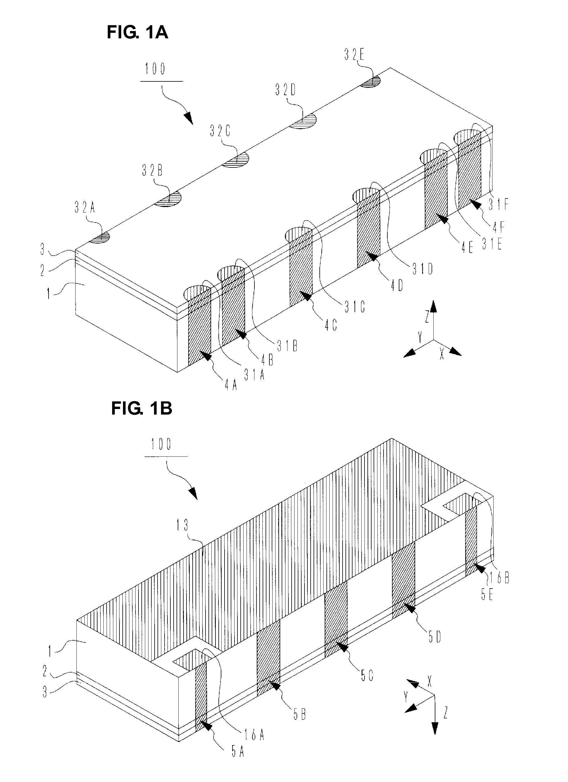
[0032]FIGS. 1A and 1B are external views of a chip component 100. FIG. 1A is a perspective view obtained by arranging the chip component 100 so that the front end thereof surfaces the front in the left of the drawing, and FIG. 1B is a perspective view obtained by rotating the chip component 100 around the Y-axis by 180 degrees from the position thereof in FIG. 1A.

[0033]The chip component 100 used in the description of the present preferred embodiment preferably is a substantially rectangular parallelepiped chip filter component in which an upper principal surface of a substantially rectangular flat plate dielectric substrate 1 is coated with a first glass layer 2 and an upper principal surface of the first glass layer is coated with a second glass layer 3. A filter is...