Semiconductor light emitting device

a light emitting device and semiconductor technology, applied in the field of semiconductor light emitting elements and light emitting devices, can solve the problems of high resistance of the element, increased voltage value (vf), and increased current spread/uniformity, and achieve the effects of reducing vf and mass productivity, improving power efficiency, and reducing resistan

Active Publication Date: 2008-06-19
NICHIA CORP
View PDF9 Cites 56 Cited by
  • Summary
  • Abstract
  • Description
  • Claims
  • Application Information

AI Technical Summary

Benefits of technology

[0019]In the light emitting element according to the present invention, the upper layer side and the lower layer side of the first electrode have respective optical properties, light transparency, and reflectivity, and located and structured preferably with the adjacent...

Problems solved by technology

In the above-mentioned related techniques, in using the transparent conductive film for the n-electrode, problems occur in terms of current spread/uniformity, high resistance of the element, and an increased voltage value (Vf).
In adopting the l...

Method used


Image

  • Semiconductor light emitting device
  • Semiconductor light emitting device
  • Semiconductor light emitting device

Examples


first embodiment

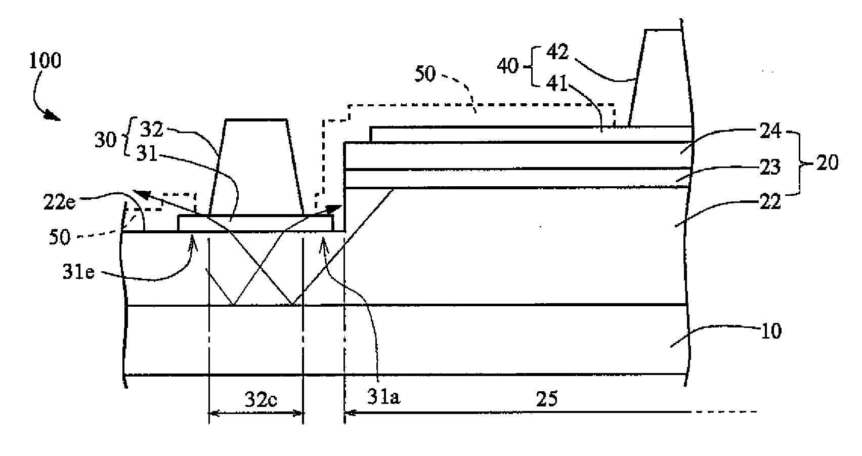
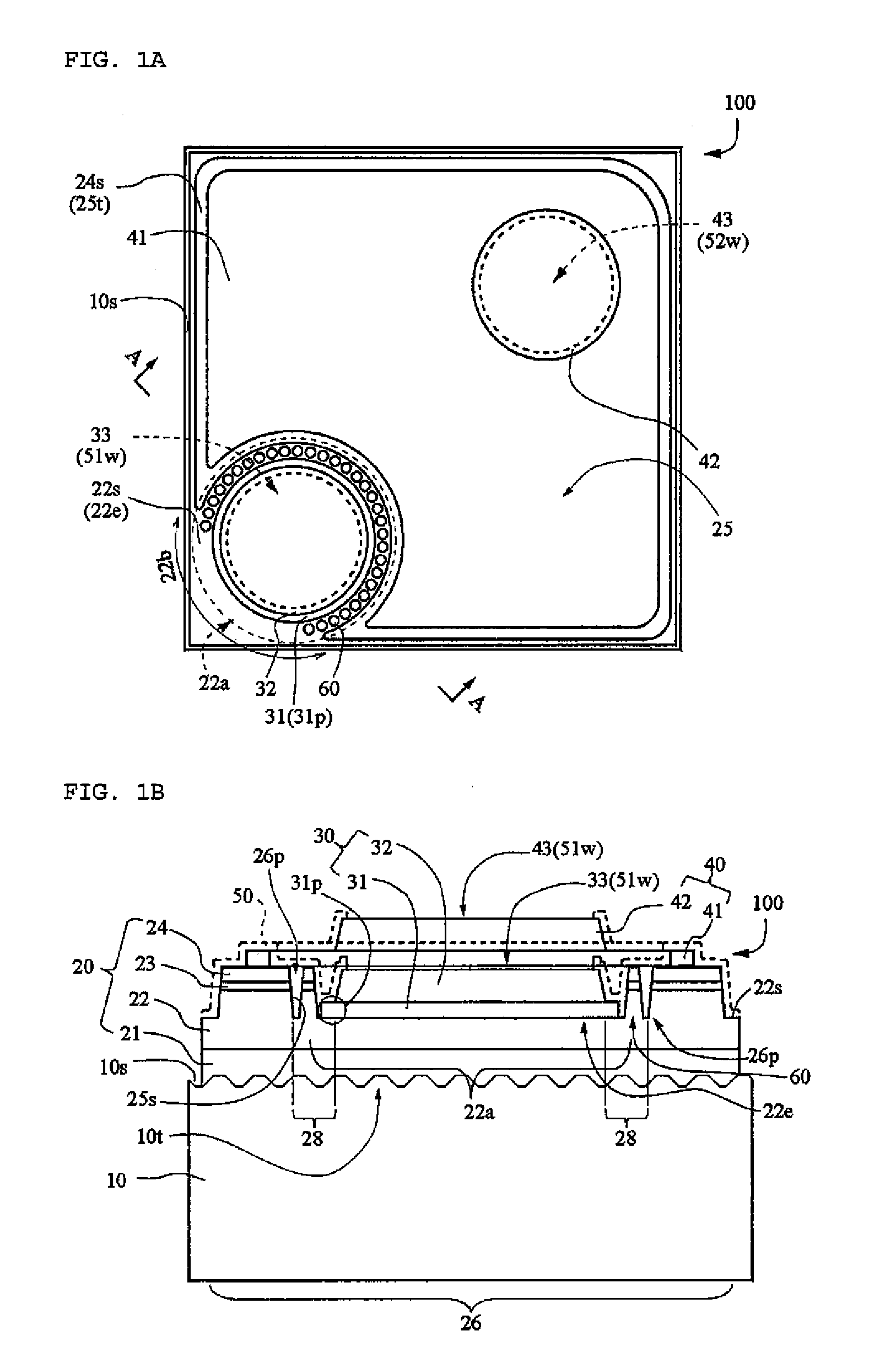
[0034]With reference to FIG. 1, a configuration of a specific example of an LED 100 according to a first embodiment is described. Here, FIG. 1A is a schematic view illustrating a plane of an LED according to the first embodiment seen from the electrode arrangement face side, and FIG. 1B is a schematic view illustrating a cross section along a line A-A of FIG. 1A.

[0035]A structure of a light emitting element of FIG. 1 is a element structure as described below. The element has a semiconductor structure 20 comprised of a lamination structure obtained by laminating an n-type nitride semiconductor layer 22 as a first conductive type layer, an active layer 23 as a light emitting portion, and a p-type nitride semiconductor layer 24 as a second conductive type layer on a substrate 10 via a underlying layer 21 such as a buffer layer. Part of the n-type layer 22 is exposed to be provided with an n-electrode (first electrode) 30. A p-electrode (second electrode) 40 is provided on a p-type laye...

second embodiment

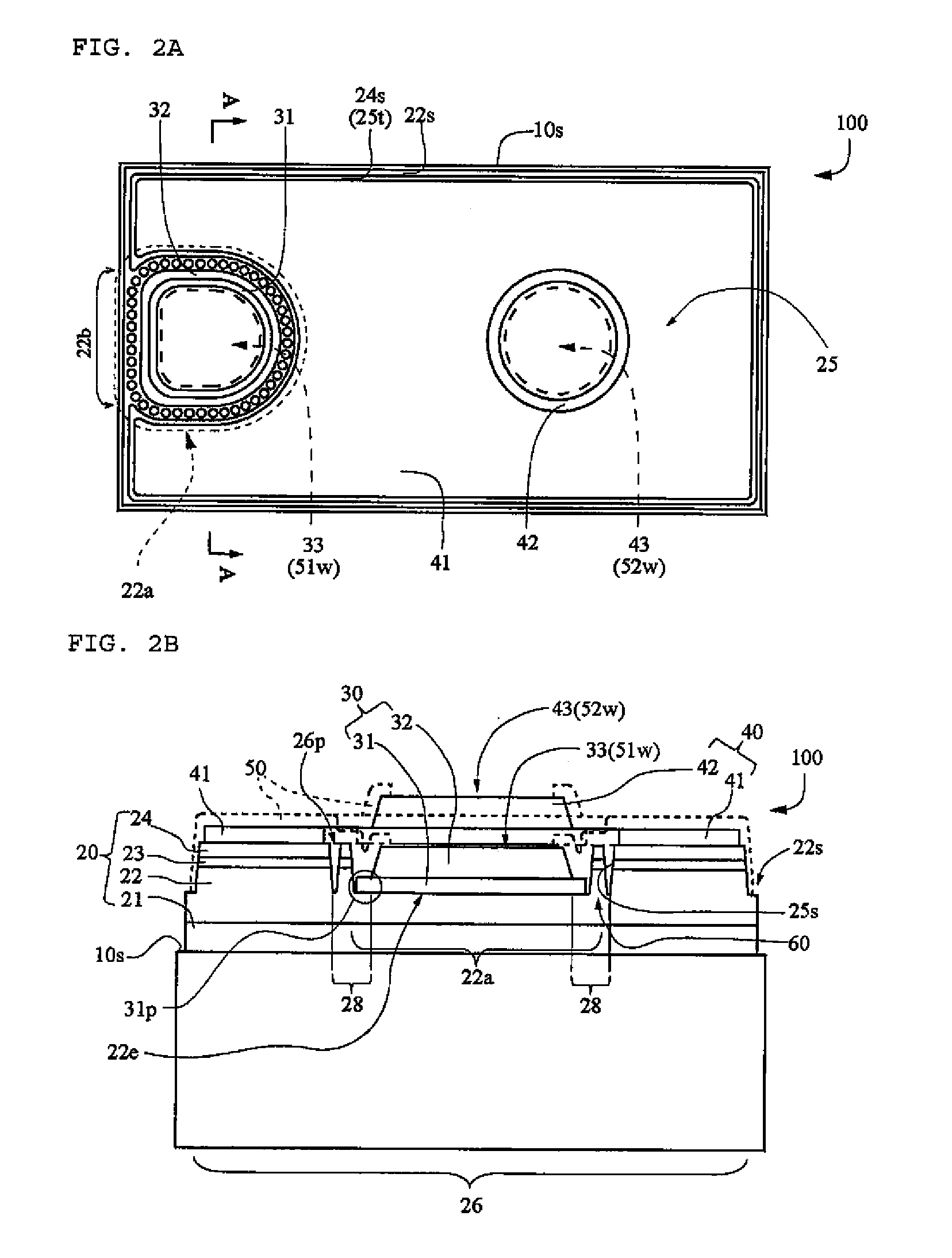
[0070]As a second embodiment, as compared with the LED formed in a substantially square shape of the specific example (FIG. 1) of the above first embodiment, an LED is formed in a rectangular shape with dimensions of 420 μm×240 μm as shown in FIG. 2. This can be produced in the same manner as in the first embodiment. FIG. 2A shows a schematic plan view of this light emitting element, and FIG. 2B shows a schematic cross-sectional view taken along the cutting surface A-A of FIG. 2A.

[0071]The depressed portion 22a of the light emitting structure 25 as the forming region 22e of the first electrode 30 is provided as a corner of the light emitting structure on one longitudinal end side of the elongated region of light emitting structure or the light emitting element. Further, the longitudinal direction is opened and the outer edge that surrounds the others is formed in the light emitting structure. Specifically, the outer edge is shaped such that one side of the rectangular electrode form...

third embodiment

[0079]In an example shown in FIG. 4, two electrode forming regions 22e and two first electrodes 30 are provided inside the light emitting structure 25, and the first electrode is arranged between the light emitting structure portion. Therefore, elongated light emitting structure portions 25A and 25B are structured to be arranged in their width directions alternately with the first electrodes (forming regions 22e), and the first electrodes 30 are structured to have the external connecting portions 33 and 43 with large widths and the extending portions 34 and 44 with narrow widths extending longitudinally from the external connecting portions 33 and 43. In this way, the structure can be formed having the first electrodes 30 arranged in parallel with the elongated light emitting structure portions 25A and 25B and the extending portion 34 of the first electrode 30, which can realize the preferable current spread and light emission. FIG. 4A is a schematic plan view of the light emitting ...


PUM


Abstract

It is an important factor in application to the illumination field and the like to obtain a characteristic excellent in power efficiency in a light emitting element. The present invention provides a semiconductor light emitting element including: first and second conductive type semiconductor layers; first and second electrodes respectively provided on the same plane sides as the first and second conductive type semiconductor layers; and a light emitting structure, provided with the second electrode and including the first and second conductive type semiconductor layers, wherein the first electrode provided on an exposed surface of the first conductive type semiconductor layer at least has a translucent first layer and a reflective second layer, and the first layer has projecting portions projected from both sides of the second layer in a cross section of the element crossing over the light emitting structure and the first electrode.

Description

[0001]This application is based on and claims priority to Japanese Patent application Nos. 2006-178652 filed on Jun. 28, 2006 and 2007-163204 filed on Jun. 20, 2007, the contents of which are incorporated hereinto by reference.BACKGROUND OF THE INVENTION[0002]1. Field of the Invention[0003]The present invention relates to a semiconductor light emitting element and a light emitting device using the same, and particularly, to an electrode structure of the light emitting element.[0004]2. Description of the Related Art[0005]A variety of researches have been made on the light emitting element using a nitride semiconductor, since light emission is obtained in the near-ultraviolet area to the red color area due to a wide band gap property of the light emitting element. A typical basic structure of the nitride semiconductor light emitting element is a structure where an n-type nitride semiconductor, an active layer and a p-type nitride semiconductor are laminated on a substrate, and respect...

Claims


Application Information

Patent Timeline
IPC IPC(8): H01L33/00H01L33/06H01L33/20H01L33/32H01L33/38H01L33/42H01L33/56H01L33/62
CPCH01L33/20H01L2924/01322H01L33/405H01L33/42H01L2224/32245H01L2224/48091H01L2224/48247H01L2224/48257H01L2224/48465H01L2224/49107H01L2224/73265H01L33/382H01L2924/3025H01L2924/00014H01L2924/00H01L2924/00012
Inventor SAKAMOTO, TAKAHIKOONISHI, MASAHIKOINOUE, YOSHIKI
Owner NICHIA CORP
Why Eureka
Try Eureka