Memory elements and cross point switches and arrays of same using nonvolatile nanotube blocks

a technology of nonvolatile nanotube blocks and memory elements, which is applied in the direction of digital storage, semiconductor devices, instruments, etc., can solve the problems of increasing cost and complexity of digital designs, reducing geometries quickly, and avoiding fet switching elements

Active Publication Date: 2008-06-19
NANTERO
View PDF77 Cites 67 Cited by
  • Summary
  • Abstract
  • Description
  • Claims
  • Application Information

AI Technical Summary

Benefits of technology

[0033]Under one aspect, a covered nanotube switch includes: (a) a nanotube element including an unaligned plurality of nanotubes, the nanotube element having a top surface, a bottom surface, and a plurality of side surfaces; (b) first and second conductive terminals in contact with the nanotube element, wherein the first conductive terminal is disposed on and substantially covering the entire top surface of the nanotube element, and wherein the second conductive terminal contacts at least a portion of the bottom surface of the nanotube element; and (c) control circuitry in electrical communication with and capable of applying electrical stimulus to the first and second conductive terminals, wherein the nanotube element is capable of switching between a plurality of electronic states in response to a corresponding plurality of electrical stimuli applied by the control circuitry to the first and second conductive terminals, and wherein, for each different electronic state of the plurality of electronic states, the nanotube element provides an electrical pathway of corresponding different resistance between the first and second conductive terminals.
[0034]One or more embodiments include one or more of the following features. The first conductive terminal is also disposed on and substantially covers at least one side surface of the plurality of side surfaces. The first conductive terminal is also disposed on and substantially covers the plurality of side surfaces. An insulator layer in contact with the bottom surface of the nanotube element, the insulator layer and the second conductive terminal together substantially covering the entire bottom surface of the nanotube element. An insulator layer in contact with at least one of the bottom surface of the nanotube element and one of the side surfaces of the nanotube element. The insulator layer includes one of SiO2, SiN, and Al2O3. A passivation layer overlying at least the first conductive terminal, the passivation layer substantially sealing the first and second conductive terminals and the nanotube element to the environment. The passivation layer includes one of SiO2, SiN, Al2O3, polyimide, phosphosilicate glass oxide, polyvinylidine fluoride, polypropylene carbonate, and polyethylene carbonate. The second conductive terminal contacts substantially the entire bottom surface of the nanotube element. The first and second conductive terminals each include a conductive material independently selected from the group consisting of Ru, Ti, Cr, Al, Al(Cu), Au, Pd, Pt, Ni, Ta, W, Cu, Mo, Ag, In, Ir, Pb, Sn, TiAu, TiCu, TiPd, PbIn, TiW, RuN, RuO, TiN, TaN, CoSix, and TiSix.
[0035]Under another aspect, a covered nanotube switch includes: (a) a nanotube element including an unaligned plurality of nanotubes, the nanotube element having top and bottom surfaces; (b) first and second conductive terminals in contact with the nanotube element and in spaced relation to each other; (c) a first insulator layer in contact with the top surface of the nanotube element; (d) a second insulator layer in contact with the bottom surface of the nanotube element, wherein the first and second conductive terminals and the first and second insulator layers together substantially surround the nanotube element; and (e) control circuitry in electrical communication with and capable of applying electrical stimulus to the first and second conductive term...

Problems solved by technology

These requirements challenging the semiconductor industry to rapidly reduce geometries using improved process features.
Integrated circuits constructed from either bipolar or FET switc...

Method used


Image

  • Memory elements and cross point switches and arrays of same using nonvolatile nanotube blocks
  • Memory elements and cross point switches and arrays of same using nonvolatile nanotube blocks
  • Memory elements and cross point switches and arrays of same using nonvolatile nanotube blocks

Examples


Embodiment Construction

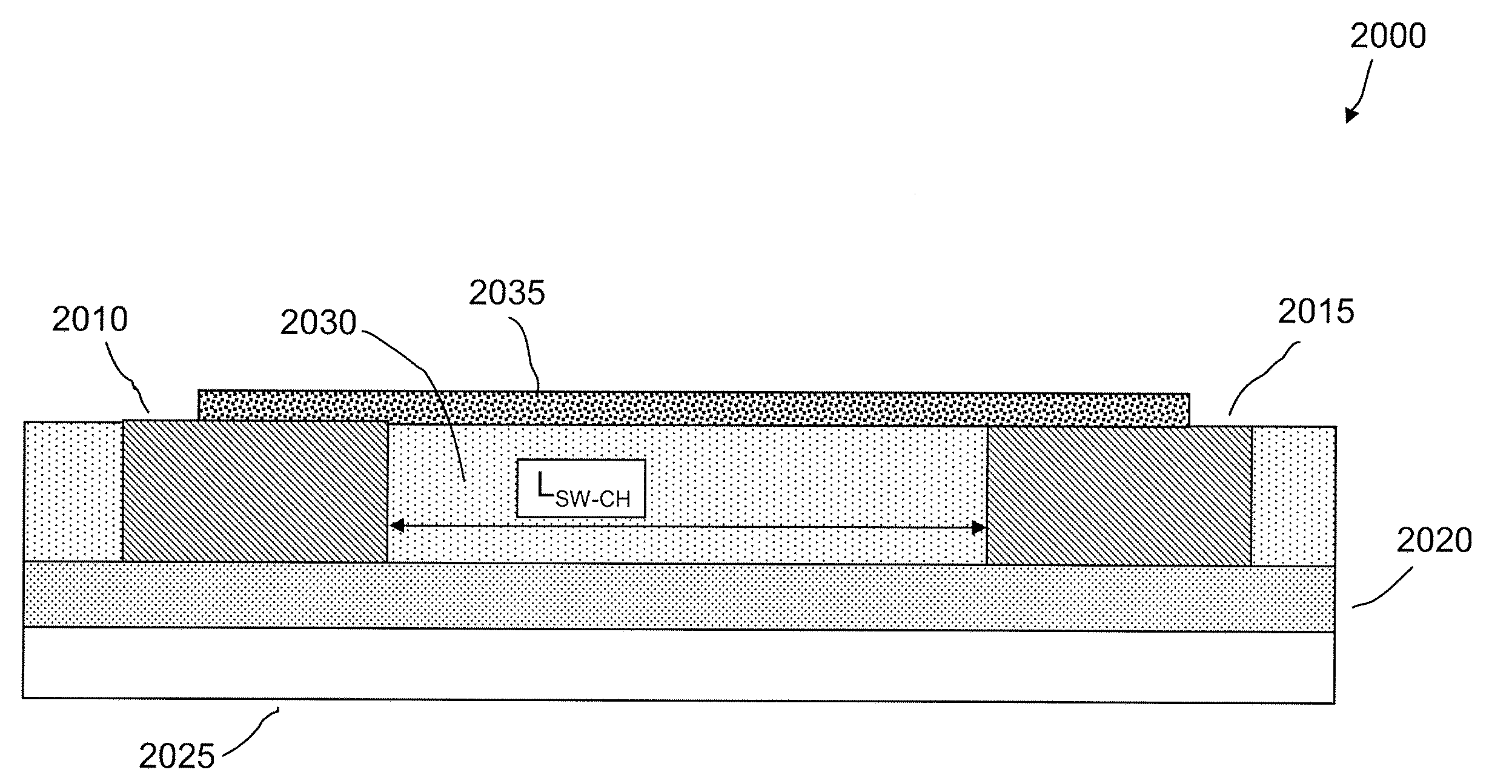
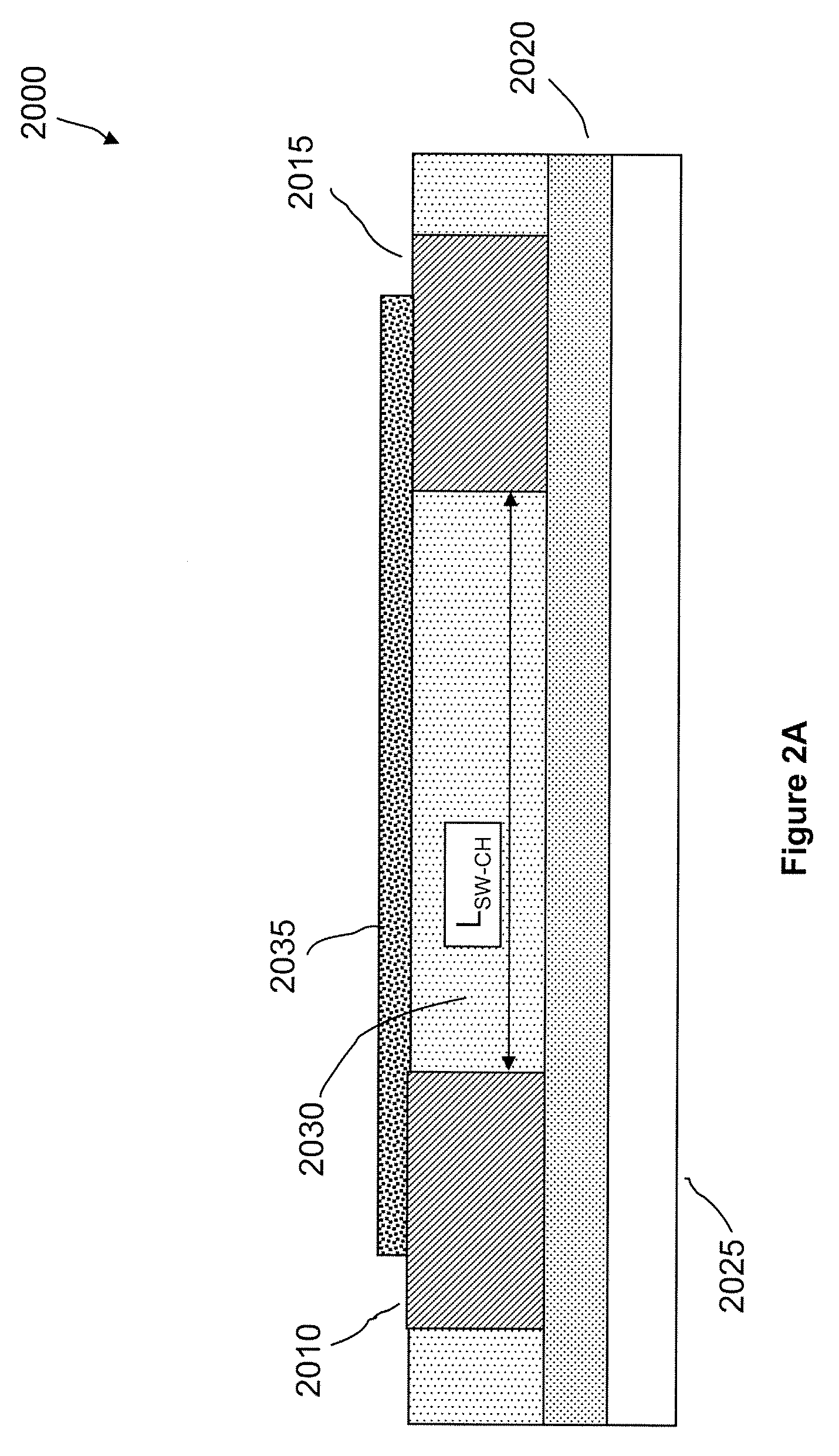
[0086]Embodiments of the invention provide memory elements and crosspoint switches and arrays of same using non-volatile nanotube blocks. The memory cells and cross point switches include two-terminal nanotube switches, which include a nanotube element such as a nanotube block, in electrical communication with two terminals. The switches are capable of repeated toggling between first and second states in response to electrical stimulus at the two terminals, and thus are capable of storing a memory state or of providing a reprogrammable electrical connection. The use of nanotube “blocks,” as contrasted with relatively thin (e.g., 0.5-10 nm) nanotube films, enables the fabrication of relatively high density memory and cross point switch arrays.

[0087]Some embodiments provide 2-D cell structures and enhanced 3-D cell structures that enable dense nonvolatile memory arrays that include two terminal nonvolatile nanotube storage nodes. The nodes include 2-D nanotube switches referred to as ...


PUM


Abstract

Under one aspect, a covered nanotube switch includes: (a) a nanotube element including an unaligned plurality of nanotubes, the nanotube element having a top surface, a bottom surface, and side surfaces; (b) first and second terminals in contact with the nanotube element, wherein the first terminal is disposed on and substantially covers the entire top surface of the nanotube element, and wherein the second terminal contacts at least a portion of the bottom surface of the nanotube element; and (c) control circuitry capable of applying electrical stimulus to the first and second terminals. The nanotube element can switch between a plurality of electronic states in response to a corresponding plurality of electrical stimuli applied by the control circuitry to the first and second terminals. For each different electronic state, the nanotube element provides an electrical pathway of different resistance between the first and second terminals.

Description

CROSS-REFERENCE TO RELATED APPLICATIONS[0001]This application claims the benefit under 35 U.S.C. §119(e) of the following applications, the entire contents of which are incorporated herein by reference:[0002]U.S. Provisional Patent Application No. 60 / 918,388, entitled “Memory Elements and Cross Point Switches and Arrays of Same Using Nonvolatile Nanotube Blocks,” filed on Mar. 16, 2007;[0003]U.S. Provisional Patent Application No. 60 / 855,109, entitled “Nonvolatile Nanotube Blocks,” filed on Oct. 27, 2006;[0004]U.S. Provisional Patent Application No. 60 / 840,586, entitled “Nonvolatile Nanotube Diode,” filed on Aug. 28, 2006;[0005]U.S. Provisional Patent Application No. 60 / 836,437, entitled “Nonvolatile Nanotube Diode,” filed on Aug. 8, 2006;[0006]U.S. Provisional Patent Application No. 60 / 836,343, entitled “Scalable Nonvolatile Nanotube Switches as Electronic Fuse Replacement Elements,” filed on Aug. 8, 2006.[0007]This application is a continuation-in-part of and claims priority under...

Claims


Application Information

Patent Timeline
IPC IPC(8): H01L29/68
CPCB82Y10/00G11C13/0021G11C13/025G11C17/16G11C17/165G11C2213/19G11C2213/77G11C2213/79H01L27/10H01L27/105H01L27/112H01L29/0665H01L29/0669H01L29/0673H01L51/0048H01L51/0591H01L27/1052Y10S977/943G11C5/063G11C13/0002G11C13/004G11C13/0069G11C2213/16G11C2213/35G11C2213/82H10B99/00H10B20/00H10K85/221H10K10/50
Inventor BERTIN, CLAUDE L.HUANG, X. M. H.RUECKES, THOMASSIVARAJAN, RAMESH
Owner NANTERO
Why Eureka
Try Eureka