Electronic apparatus

a technology of electronic equipment and resonant antennas, applied in the direction of resonant antennas, independent non-interaction antenna combinations, protective material radiating elements, etc., can solve the problems of space required and become difficult to ensure such a spa

Active Publication Date: 2008-06-26
KK TOSHIBA
View PDF7 Cites 60 Cited by
  • Summary
  • Abstract
  • Description
  • Claims
  • Application Information

AI Technical Summary

Benefits of technology

[0005]In an electronic apparatus such as a cellular phone or PDA (Personal Digital Assistant), for suppressing affection of noise between an antenna and circuit components, it is preferable that they are disposed so that the distance thereof becomes long as much as possible. For example, there is a structure in which an antenna by in-mold or MID (Molded Interconnection Device) is separated from the substrate and disposed between the substrate provided with the circuit components and the housing and in which the power supply between the antenna and the substrate is performed through a plate spring or a spring connector or the like.

Problems solved by technology

However, for disposing a plate spring or a spring connector, a space is required.
As downsizing, thinning, and weight saving of the electronic apparatus are more required and substrate package density is higher, it becomes difficult to ensure such a space.

Method used


Image

  • Electronic apparatus
  • Electronic apparatus
  • Electronic apparatus

Examples


first embodiment

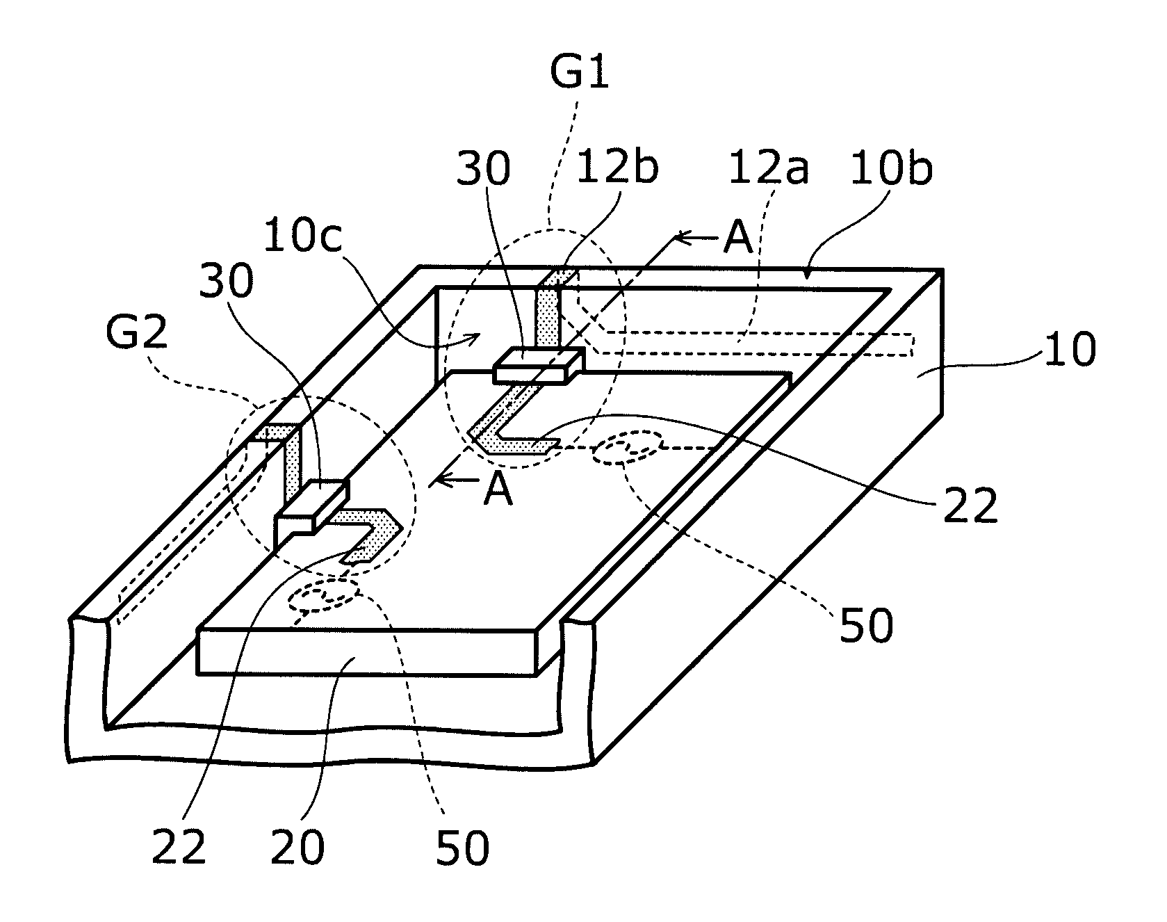
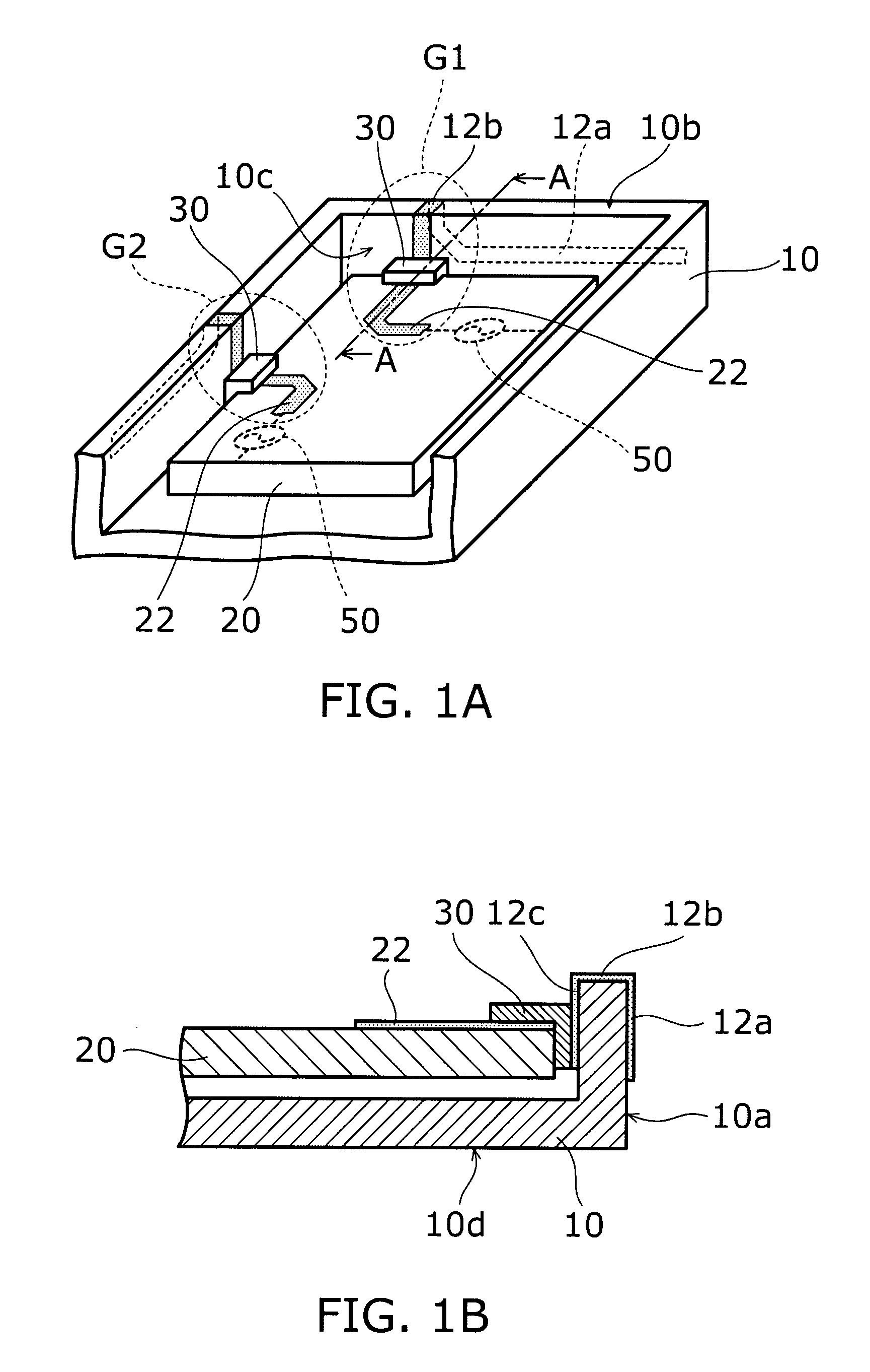
[0023]FIGS. 1A and 1B show an electronic apparatus according to this invention. FIG. 1A is a schematic perspective view, and FIG. 1B is a schematic section view along the chain line A-A. A housing 10 may be any one of an operating portion including a keyboard and a display portion including a liquid crystal image. A surface of the housing 10 having a frame portion is composed of an outer surface and an inner surface.

[0024]Out of them, the outer surface includes a frame outer surface portion 10a and a bottom surface portion 10d, and the inner surface includes a frame upper surface portion 10b and a frame inner surface portion 10c. An antenna pattern 12 includes 12a provided on the frame outer surface portion 10a, 12b provided on the frame upper surface portion 10b, and 12c provided on the inner surface portion 10c.

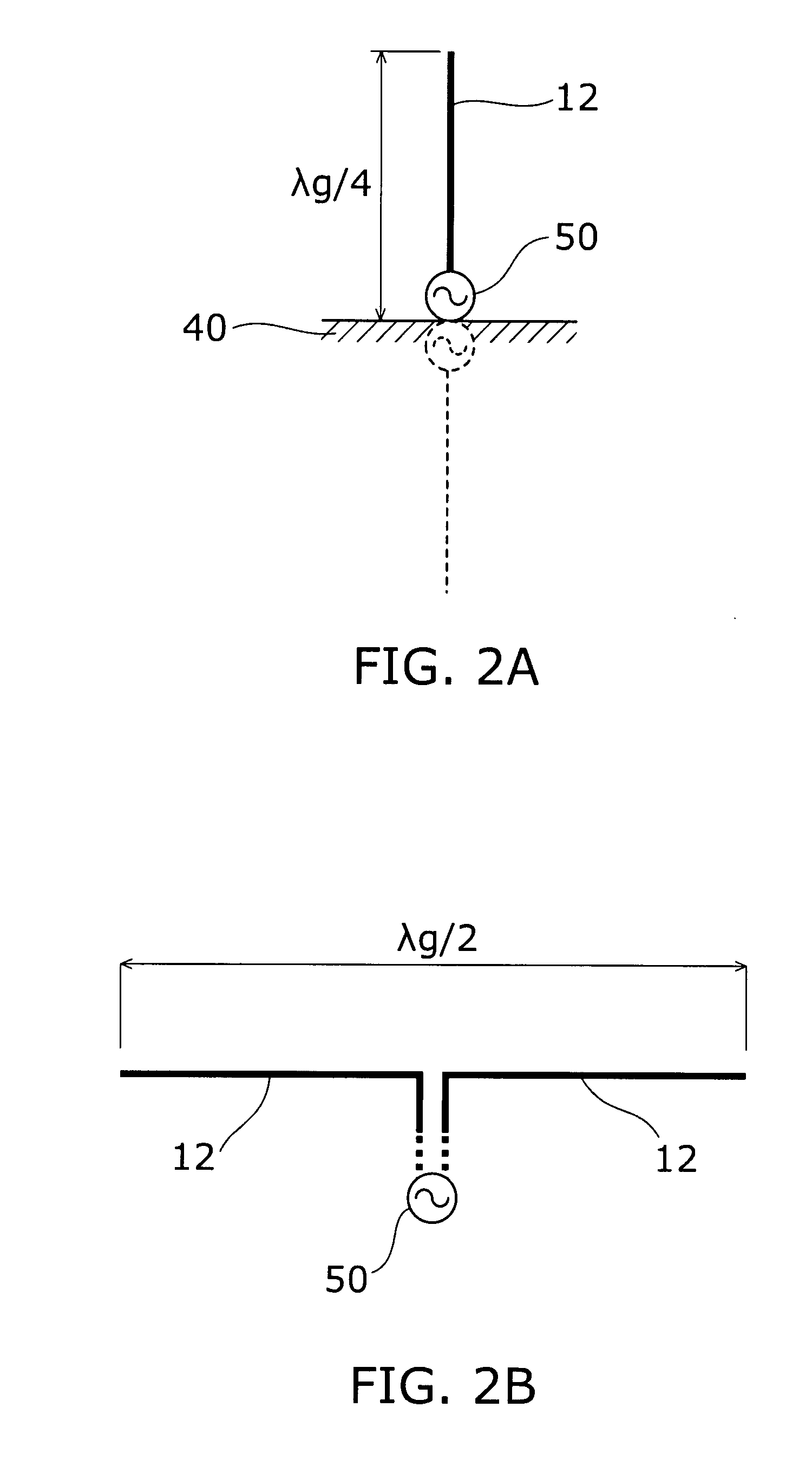
[0025]When the antenna pattern 12a is made to extend onto the frame outer surface portion 10a of the housing 10, the distance from circuit components (not shown) on a subs...

second embodiment

[0039]FIGS. 4A and 4B show an electronic apparatus according to this invention. FIG. 4A is a schematic perspective view, and FIG. 4B is a schematic section view along the chain line AA. The same components as FIGS. 1A and 1B are appended with the same number and specific explanation thereof will be omitted. The wiring layer 22 on the substrate 20 is connected to the antenna pattern 12c through a conductive member 32 composed of a sheet metal or the like. The conductive member 32 of a sheet metal is fixed to the housing 10 with a screw 34 or the like. Adhesion is also possible without using a screw. Also, welding is possible without using a screw, similarly. As an example of the welding, there is a method of providing a protruding part in the housing, fitting the protruding part into the conductive member having a protruding portion, and heating to melt down the protruding part and thereby to perform the fixation.

[0040]In this case, the conductive member 32 contacts the wiring layer ...

third embodiment

[0042]FIGS. 5A and 5B show an electronic apparatus according to this invention. FIG. 5A is a schematic perspective view, and FIG. 5B is a schematic section view along the chain line AA.

[0043]A conductive layer 22c is a portion of the wiring layer 22 formed on a surface of the substrate 20 which extends onto the side surface of the substrate 20. The substrate 20 is pressed to the inner surface portion 10c of the housing 10, and the conductive layer 22c and the antenna pattern 12c are contacted, and thereby, favorable electric contact is formed. The structure is simple, but downsizing and thinning of the housing 10 are possible with maintaining the antenna performance.

[0044]As described above, electrical connection between the antenna pattern 12 and the wiring layer 22 on the substrate 20 has been explained. Next, a method of fixation between the substrate 20 and the housing 10 will be explained. For fixing the substrate 20 to the housing 10, screw cramp, adhesion, welding, or the lik...


PUM


Abstract

An electronic apparatus includes: a housing provided with a first conductive pattern; a substrate provided with a first wiring layer in a surface thereof and fixed to the housing; and a first conductive member connecting the first conductive pattern and the first wiring layer. The first conductive pattern extends onto an outer surface and an inner surface of the housing. The first conductive member is in contact with each of at least a part of the first conductive pattern extending onto the inner surface and an end of the first wiring layer. Alternatively, an electronic apparatus includes: a housing provided with a conductive pattern and having a through part in a frame portion thereof; and a substrate provided with a wiring layer on a surface thereof and having a protruding part and fixed to the housing. The protruding part and the through part are fit. The conductive pattern extends onto an outer surface of the housing and onto an inner surface of the through part. At least some of the conductive pattern extending onto the inner surface is in contact with an end of the wiring layer.

Description

CROSS-REFERENCE TO RELATED APPLICATIONS[0001]This application is based upon and claims the benefit of priority from the prior Japanese Patent Application No. 2006-343486, filed on Dec. 20, 2006; the entire contents of which are incorporated herein by reference.BACKGROUND OF THE INVENTION[0002]1. Field of the Invention[0003]This invention relates to an electronic apparatus.[0004]2. Background Art[0005]In an electronic apparatus such as a cellular phone or PDA (Personal Digital Assistant), for suppressing affection of noise between an antenna and circuit components, it is preferable that they are disposed so that the distance thereof becomes long as much as possible. For example, there is a structure in which an antenna by in-mold or MID (Molded Interconnection Device) is separated from the substrate and disposed between the substrate provided with the circuit components and the housing and in which the power supply between the antenna and the substrate is performed through a plate sp...

Claims


Application Information

Patent Timeline
Patent Type & Authority Applications(United States)
IPC IPC(8): H01Q1/22H01L25/00H01Q1/24H01Q1/38H04B1/38H04B1/3822H05K7/14
CPCH01Q9/40H01Q9/42H01Q21/28H05K1/0284H05K2203/167H05K3/325H05K2201/048H05K2201/0999H05K1/144
Inventor HONDA, TOMOKOKUROIWA, NOBUYOSHINAKAHATA, MASAOMIMORIMOTO, JUNHONDA, SATORUHATA, YOSHIKAZUSATO, KOICHITSUJIMURA, AKIHIROTABATA, MAKOTOSAKURAI, MINORUKATO, SHOJI
Owner KK TOSHIBA
Why Eureka
Try Eureka