Semiconductor device having shield structure

a shield structure and semiconductor technology, applied in the direction of electrical equipment, basic electric elements, waveguides, etc., can solve the problems of difficult structure of signal lines, high density, difficult to achieve effective, etc., to achieve reliably stabilize the potential of signal lines, reduce the chip size of the semiconductor device, and densely arrange the effect of the structur

Inactive Publication Date: 2009-09-24
LONGITUDE LICENSING LTD
View PDF10 Cites 18 Cited by
  • Summary
  • Abstract
  • Description
  • Claims
  • Application Information

AI Technical Summary

Benefits of technology

[0012]As described above, according to the present invention, the signal lines for transmitting a signal to be stabilized at a predetermined voltage are formed so that a shield structure is employed where the shield lines are adjacent to the signal lines in the two wring layers and the signal line in the lower wiring layer is connected to the gate electrode opposed in the stacking direction. Thus, the signal line in the lower wiring layer is connected to the gate electrode to function as a capacitor in addition to the shielding effect of the shiel

Problems solved by technology

However, only three signal lines 103 for the reference signal can be arranged within a range shown in FIG. 7, it is structurally difficult to arrange the signal lines 103 in a high density.
In this manner, when forming the shield structure by arranging a large number of the shield lines 104 for the reference signal in the above conventional semiconductor device 100, there is a problem

Method used


Image

  • Semiconductor device having shield structure
  • Semiconductor device having shield structure
  • Semiconductor device having shield structure

Examples


first embodiment

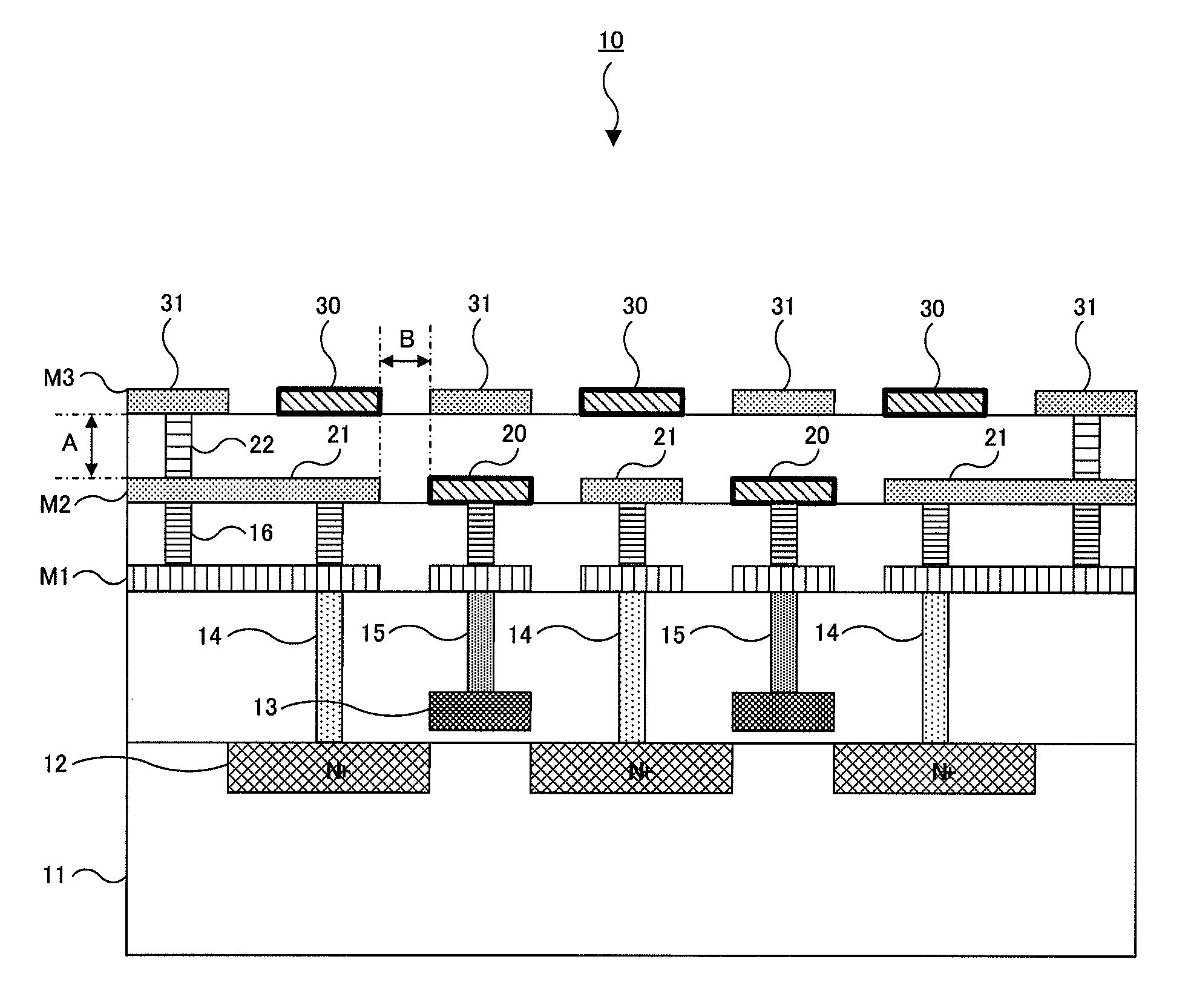
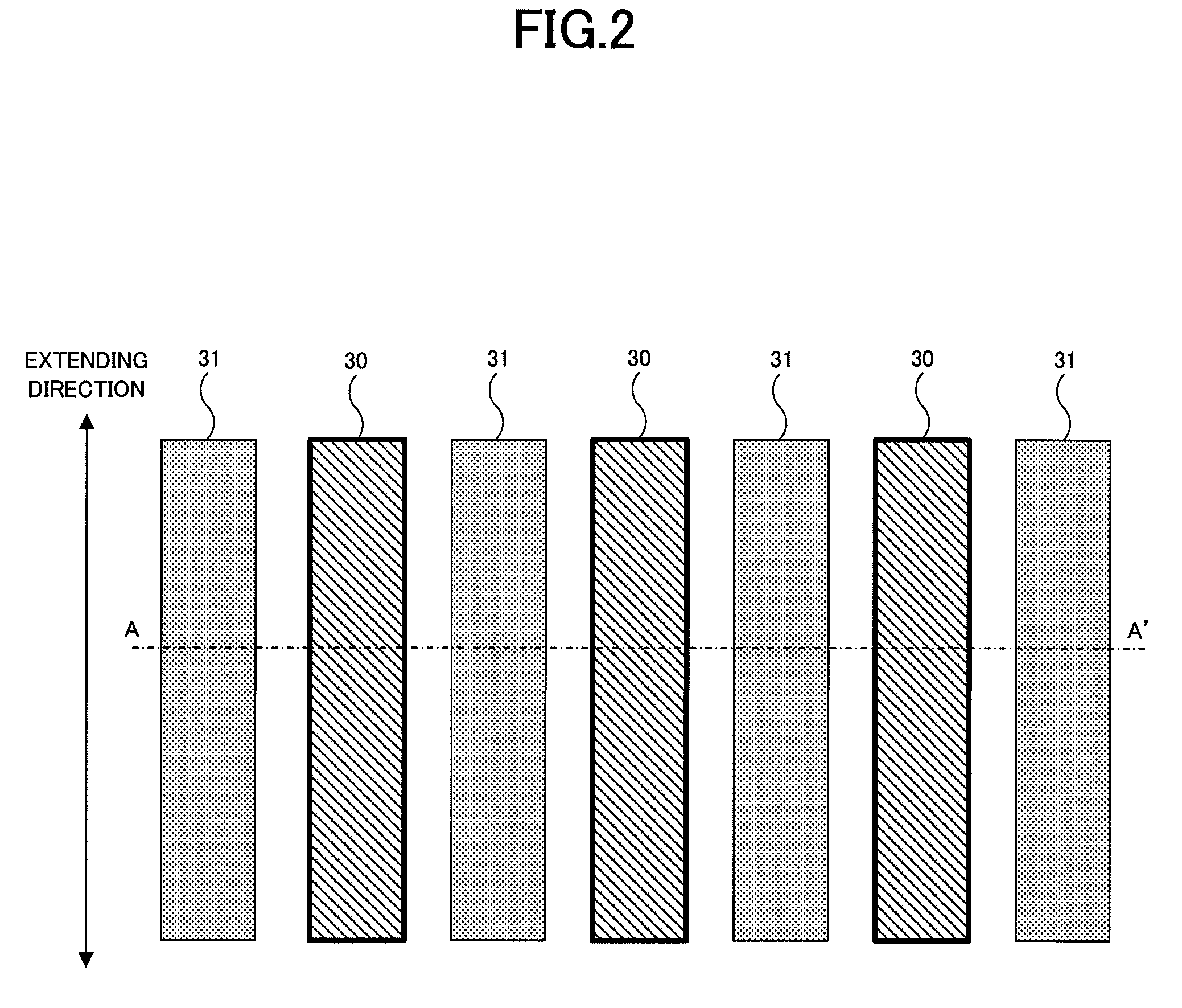
[0022]A semiconductor device of a first embodiment of the present invention will be described with reference to FIGS. 1 and 2. FIG. 1 shows a cross-sectional view of a semiconductor device 10 of the first embodiment. FIG. 2 is a plane view showing only an uppermost wiring layer M3 in the semiconductor device 10 of FIG. 1, and a cross section along A-A′ line in FIG. 2 corresponds to FIG. 1. In FIG. 2, respective lines are assumed to be arranged so as to extend in a direction of arrows.

[0023]As shown in FIG. 1, in the semiconductor device 10 of the first embodiment, N-type diffusion layers 12 are formed on a semiconductor substrate 11 made of P-type silicon. Gate electrodes 13 are formed over channels between the N-type diffusion layers 12. Gate insulating films are formed using silicon dioxide films (SiO2) between the gate electrodes 13 and the semiconductor substrate 11. Each N-type diffusion layer 12 and each gate electrodes 13 form a MOS structure in the semiconductor device 10.

[0...

second embodiment

[0038]Next, a semiconductor device of a second embodiment of the present invention will be described with reference to FIG. 5. FIG. 5 shows a cross-sectional view of the semiconductor device 10 of the second embodiment. In FIG. 5, elements common to those in the first embodiment are represented by the same numbers and description thereof will be omitted. The second embodiment differs from the first embodiment in that the lower wiring layer M2 is utilized for a purpose other than the signal lines 20 for the reference signal.

[0039]In FIG. 5, the signal line 20 for the reference signal is arranged at the right of two positions corresponding to the two signal lines 20 of the wiring layer M2 of FIG. 1, while a power supply line 23 for supplying a supply voltage VCC is arranged at the left of the two positions. This power supply line 23 is used to supply the supply voltage VCC to internal circuit elements of the semiconductor device 10. In addition, the three shield lines 21 formed in the...

third embodiment

[0043]Next, a semiconductor device of a third embodiment of the present invention will be described with reference to FIG. 6. FIG. 6 shows a cross-sectional view of the semiconductor device 10 of the third embodiment. In FIG. 6, elements common to those in the first embodiment are represented by the same numbers and description thereof will be omitted. The third embodiment differs from the first embodiment in terms of a structure of the semiconductor device 10. That is, the semiconductor device 10 of the third embodiment includes an N-type well 17 formed in the P-type substrate 11. The N-type well 17 is previously formed by adding N-type impurity such as phosphorus to an upper portion of the semiconductor substrate 11.

[0044]As shown in FIG. 6, the gate electrodes 13 are opposed to a surface of the lower semiconductor substrate 11 within a range where the N-type well 17 is formed. In this case, conductivity type of the semiconductor substrate 11 opposite to the gate electrodes 13 is ...


PUM


Abstract

A semiconductor device comprises a semiconductor substrate; a diffusion layer formed on the semiconductor substrate; at least two wiring layers formed opposite to each other over the semiconductor substrate; signal lines for transmitting a signal maintaining a predetermined voltage, each of the signal lines being formed in each of the two wiring layers; shield lines fixed to a constant voltage to shield the signal lines, each of the shield lines being formed adjacent to each of the signal lines in the two wiring layers; and a gate electrode formed over the semiconductor substrate via an insulation film. In the semiconductor device, at least one of the signal lines formed in a lower wiring layer of the at least two wiring layers is electrically connected to the gate electrode opposed in a stacking direction.

Description

BACKGROUND OF THE INVENTION[0001]1. Field of the Invention[0002]The present invention relates to a semiconductor device having signal lines for a reference signal supplied to an internal circuit, and particularly relates to a semiconductor device having a shield structure for shielding the signal lines for the reference signal from noise and the like.[0003]2. Description of Related Art[0004]Generally, a reference signal is used in a semiconductor device in order to supply a reference voltage to internal circuits. The voltage value of the reference signal is required to be stable with a small fluctuation. It is desirable to design the semiconductor device having a structure in which signal lines for transmitting the reference signal are hardly affected by other adjacent signal lines. A semiconductor device has been conventionally proposed in which a shield structure surrounding the signal lines for the reference signal is formed so as to shield the lines from the noise affected by ot...

Claims


Application Information

Patent Timeline
IPC IPC(8): H01P3/08
CPCH01P3/003
Inventor ONDA, TAKAMITSUMATSUKI, KAZUHIKO
Owner LONGITUDE LICENSING LTD
Why Eureka
Try Eureka