Eureka AIR delivers breakthrough ideas for toughest innovation challenges, trusted by R&D personnel around the world.

Stackable integrated circuit package system with recess

Active Publication Date: 2008-07-03
STATS CHIPPAC LTD
View PDF27 Cites 26 Cited by
  • Summary
  • Abstract
  • Description
  • Claims
  • Application Information

AI Technical Summary

Problems solved by technology

However, integrated circuit density continues to be limited by the “real estate” available for mounting individual integrated circuits on a substrate.
However, such multi-chip modules can be bulky.
Multi-chip packages with stacking configurations may also present problems.
Conventional spacer and packaged integrated circuits interface perform poorly in reliability test from the delamination at this interface.
Combining them into a single horizontal layer used board space inefficiently by consuming large no-lead leadframe areas, and afforded less advantage in circuit miniaturization.
However, multi-chip modules, whether vertically or horizontally arranged, can also present problems because they usually must be assembled before the component chips and chip connections can be tested.
That is, because the electrical bond pads on a die are so small, it is difficult to test die before assembly onto a no-lead leadframe.
With conventional multi-chip modules, however, the die cannot be individually identified as KGD before final assembly, leading to KGD inefficiencies and assembly process problems including yield.
Solutions to these problems have been long sought but prior developments have not taught or suggested any solutions and, thus, solutions to these problems have long eluded those skilled in the art.

Method used


Image

  • Stackable integrated circuit package system with recess
  • Stackable integrated circuit package system with recess
  • Stackable integrated circuit package system with recess

Examples


Embodiment Construction

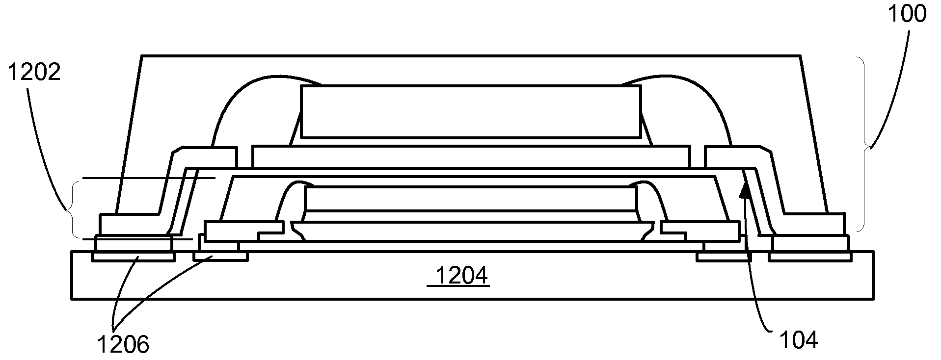
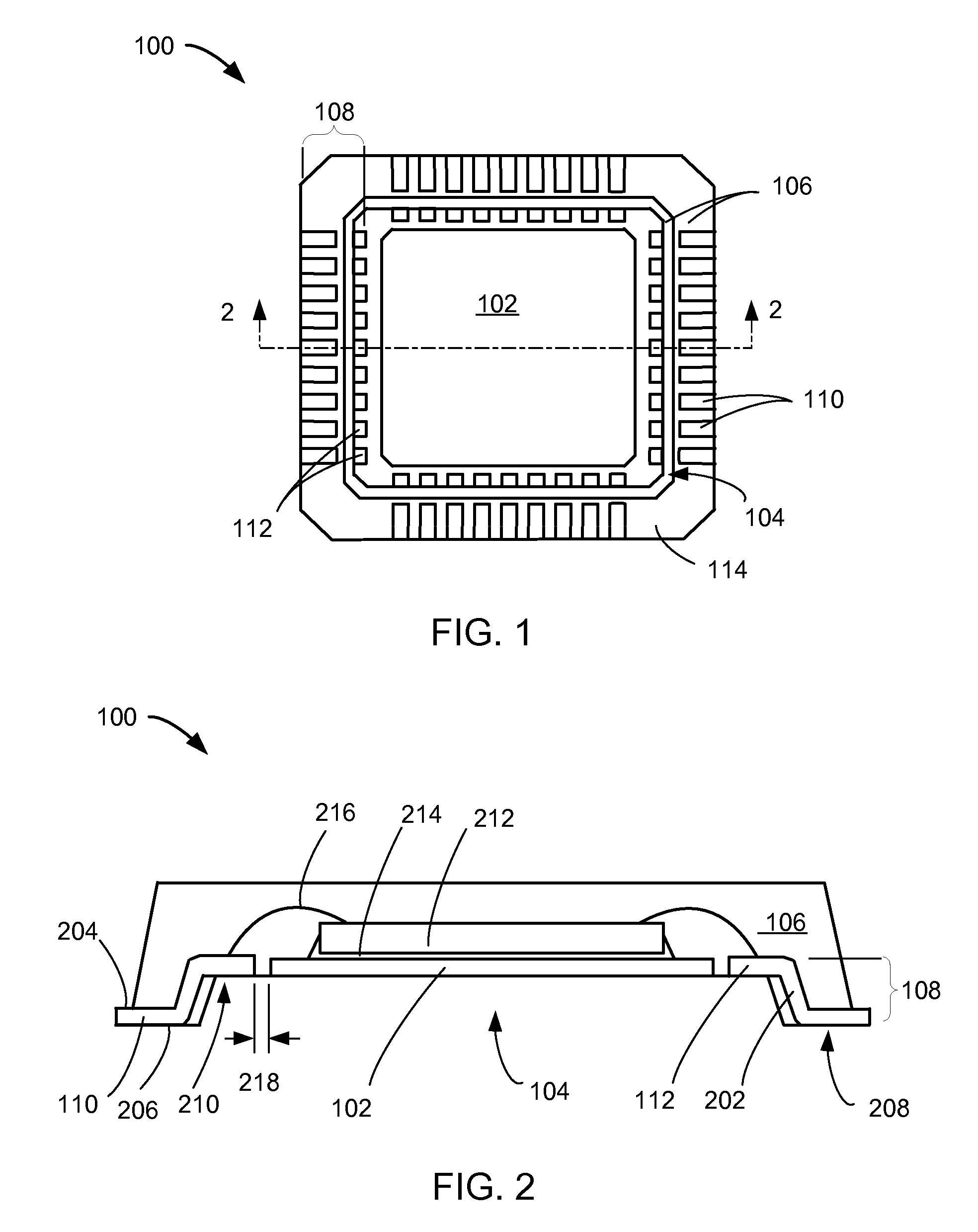
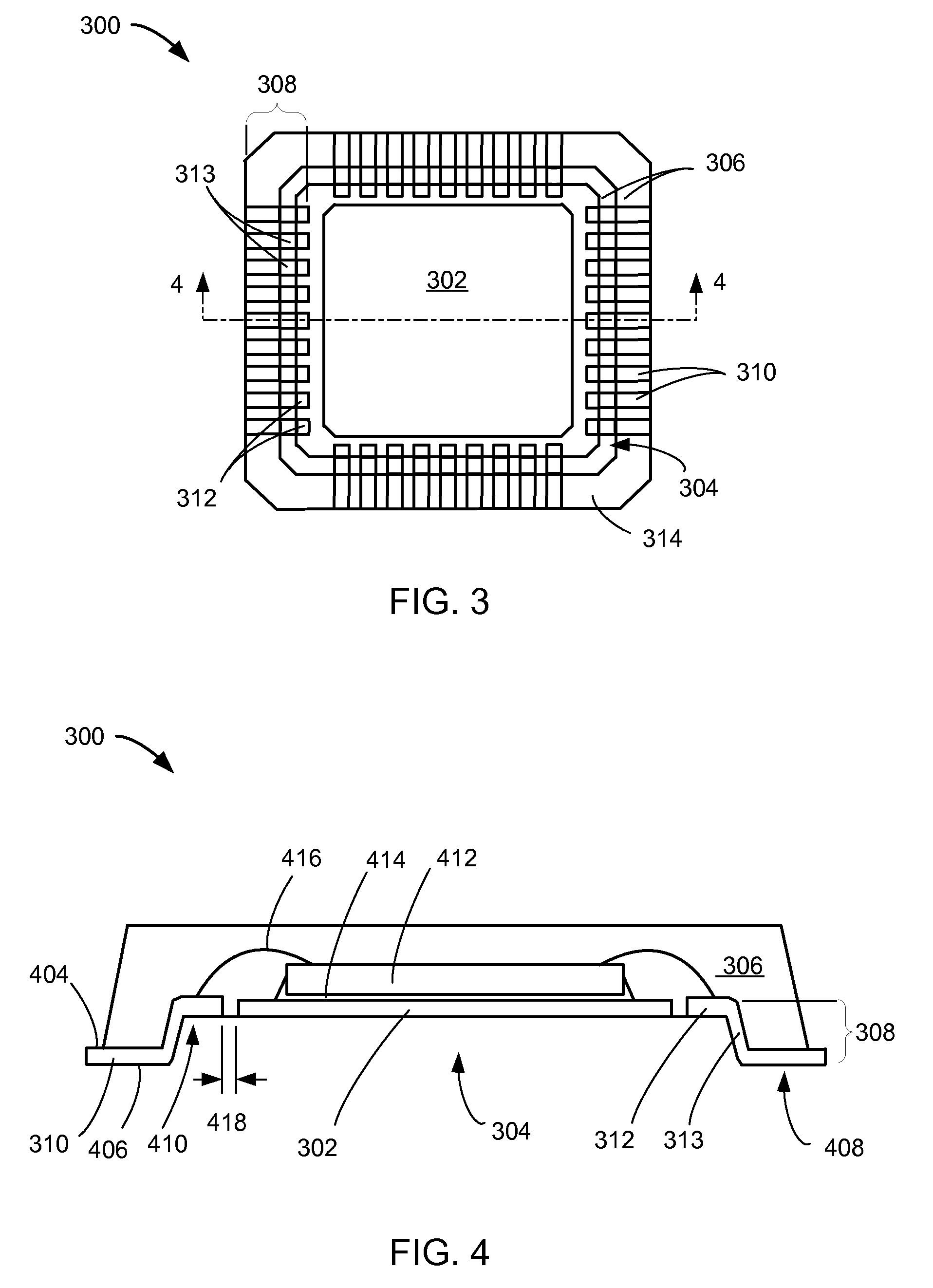
[0043]The following embodiments are described in sufficient detail to enable those skilled in the art to make and use the invention. It is to be understood that other embodiments would be evident based on the present disclosure, and that system, process, or mechanical changes may be made without departing from the scope of the present invention.

[0044]In the following description, numerous specific details are given to provide a thorough understanding of the invention. However, it will be apparent that the invention may be practiced without these specific details. In order to avoid obscuring the present invention, some well-known circuits, system configurations, and process steps are not disclosed in detail. Likewise, the drawings showing embodiments of the system are semi-diagrammatic and not to scale and, particularly, some of the dimensions are for the clarity of presentation and are shown greatly exaggerated in the drawing FIGs. In addition, where multiple embodiments are disclos...


PUM


Abstract

A stackable integrated circuit package system is provided including forming an external interconnect having an interconnect non-recessed portion and an interconnect recessed portion, mounting an integrated circuit die over a paddle that is coplanar with the interconnect recessed portion, and forming an encapsulation having a recess over the external interconnect and the integrated circuit die with the external interconnect exposed at a side of the encapsulation.

Description

CROSS-REFERENCE TO RELATED APPLICATION[0001]The present application contains subject matter related to co-pending U.S. patent application Ser. No. 11 / 164,088 filed Nov. 10, 2005. The related application is assigned to STATS ChipPAC Ltd.TECHNICAL FIELD[0002]The present invention relates generally to wafer manufacturing system and more particularly to semiconductor manufacturing system.BACKGROUND ART[0003]Integrated circuit packaging technology has seen an increase in the number of integrated circuits mounted on a single circuit board or substrate. The new packaging designs are more compact in form factors, such as the physical size and shape of an integrated circuit, and providing a significant increase in overall integrated circuit density. However, integrated circuit density continues to be limited by the “real estate” available for mounting individual integrated circuits on a substrate. Even larger form factor systems, such as personal computers, compute servers, and storage serve...

Claims


Application Information

Patent Timeline
IPC IPC(8): H01L23/02
CPCH01L21/6835H01L2924/12041H01L23/3128H01L23/49551H01L23/49555H01L23/49575H01L24/97H01L25/105H01L2224/48091H01L2224/48247H01L2224/73265H01L2224/97H01L2924/01027H01L2924/01082H01L2924/14H01L2924/1532H01L2924/3025H01L23/3107H01L25/03H01L2225/1005H01L2225/1094H01L24/48H01L2224/32245H01L2924/01033H01L2924/1815H01L2225/107H01L2225/1029H01L2924/00014H01L2924/00H01L2924/181H01L2224/45014H01L2924/00012H01L2224/45015H01L2924/207H01L2924/206
Inventor CAMACHO, ZIGMUND RAMIREZBATHAN, HENRY D.CAPARAS, JOSE ALVINTAY, LIONEL CHIEN HUI
Owner STATS CHIPPAC LTD
Why Eureka
Eureka Blog
Learn More