Integrated module of antenna and connector

Inactive Publication Date: 2008-07-03
P-TWO INDUSTRIES INC
3 Cites 7 Cited by

AI-Extracted Technical Summary

Problems solved by technology

However, in these ways, designs of signal feed-in and grounding connection regarding planar antennas become complicated.
This makes desi...

Benefits of technology

[0006]Accordingly, an object of the present invention is to provide an integrated module of antenna and connector which integrates a wideba...

Abstract

An integrated module of antenna and connector has an insulative housing receiving a plurality of conductive terminals therein, a metal shell shielding the insulative housing, and a coupling device assembled on the metal shell. The metal shell is grounded and defines a slot with a particular shape. A feed-in terminal is provided on a side of the slot and includes a soldering portion and a contact portion. The soldering portion of the feed-in terminal connects with a circuit board. The coupling device contacts the contact portion of the feed-in terminal, feeding in high-frequency voltage which forms voltage difference relative to a plane of the slot. A resonant electromagnetic field is produced in the slot for working as an antenna for electromagnetic wave radiation. Thus, functions of an antenna and a connector are combined, reducing the occupied space and decreasing the cost.

Application Domain

Antenna supports/mountingsAntennas earthing switches association +1

Technology Topic

Electromagnetic fieldVoltage +3

Image

  • Integrated module of antenna and connector
  • Integrated module of antenna and connector
  • Integrated module of antenna and connector

Examples

  • Experimental program(1)

Example

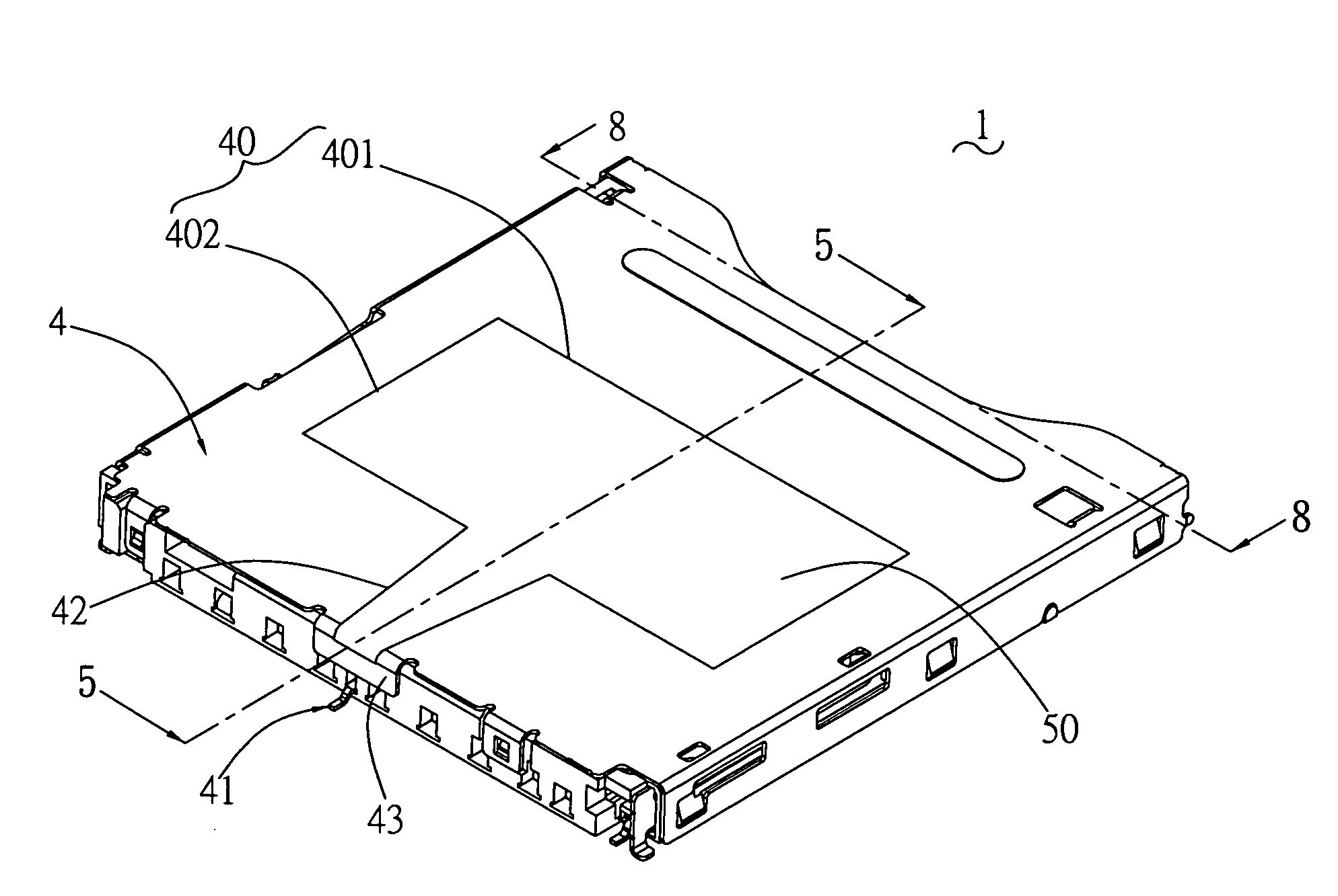
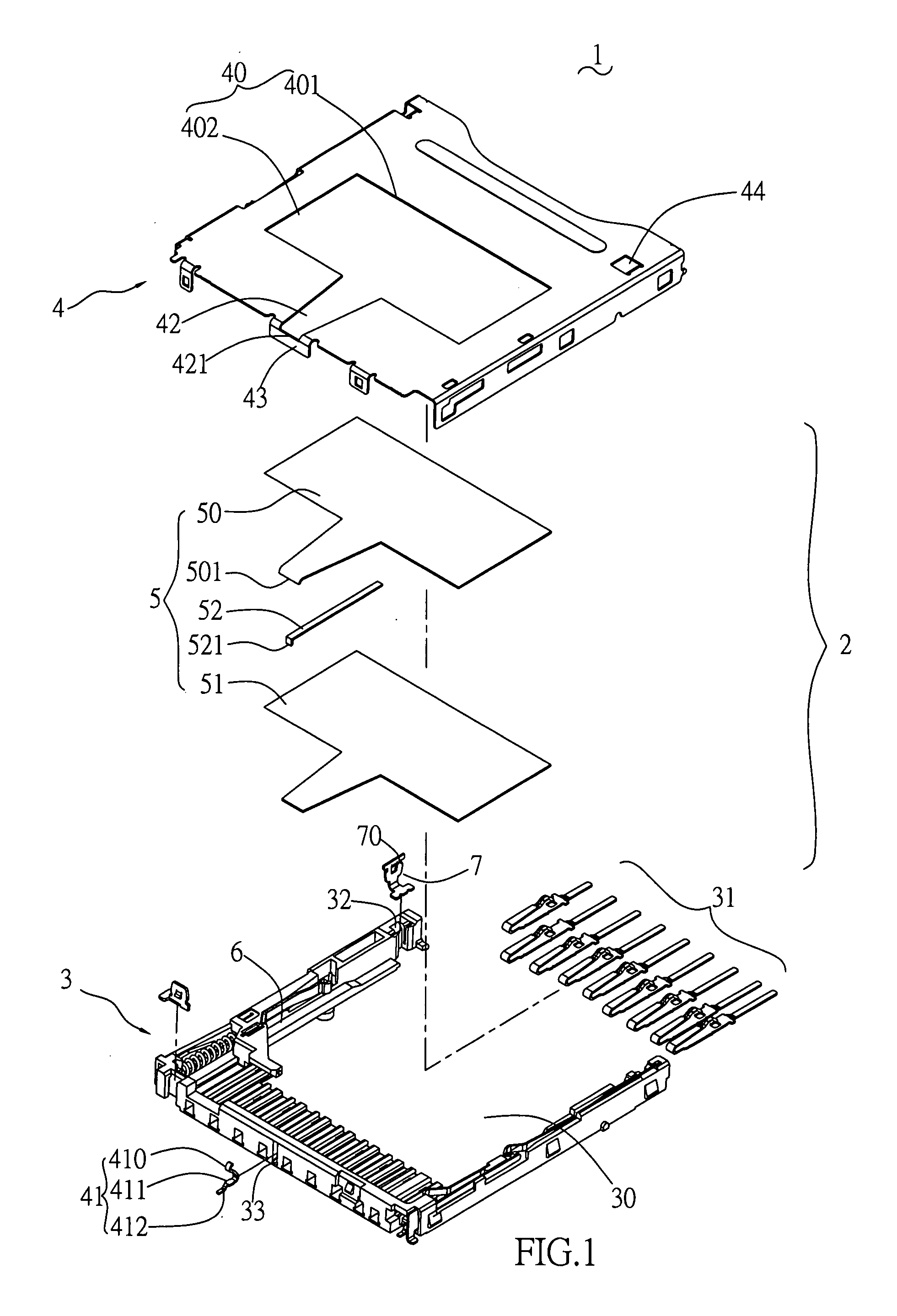
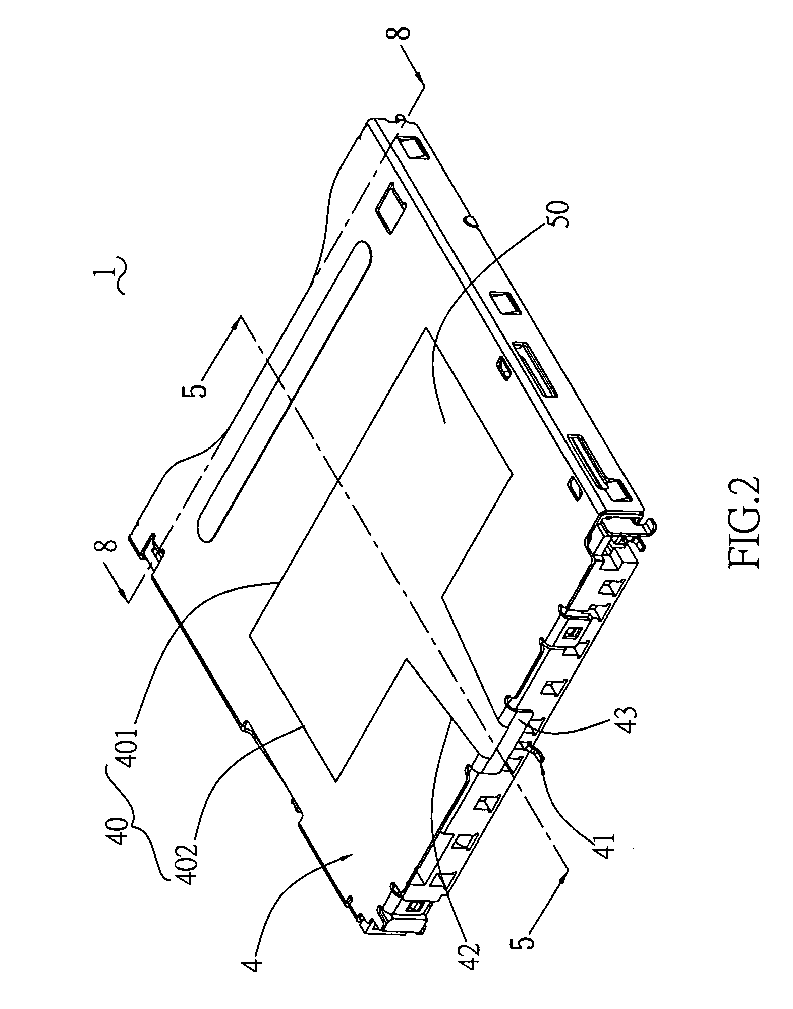
[0019]FIGS. 1 to 3 illustrate an integrated module of antenna and connector in accordance with the first embodiment of the present invention. The integrated module of antenna and connector is integrated with a memory card connector in this embodiment. The integrated module of antenna and connector 2 comprises an insulative housing 3, a metal shell 4 and a coupling device 5 assembled on the metal shell 4. The insulative housing 3 defines an opening 30 for receiving a memory card (not shown) and a plurality of conductive terminals 31. T integrated module of antenna and connector 2 further comprises an ejecting mechanism 6, which is well known in the art and does not need detailed description.
[0020]The metal shell 4 shields the insulative housing 3, and defines a rectangular slot 40 in a center thereof. The slot 40 has a pair of long sides 401 and a pair of short sides 402. A feed-in terminal 41 is provided on a long side 401. Further referring to FIG. 4, the feed-in terminal 41 includes a contact portion 410, a soldering portion 412, and an interferential portion 411 formed integrally between contact portion 410 and the soldering portion 412. The soldering portion 412 appropriately bends for surface mounting to a circuit board (not shown). With reference to FIG. 6, the contact portion 410 extends from the soldering portion 412 for contacting a contact surface 521 of a metal strip 52 of a coupling device 5 in assembly. The interferential portion 411 is interferentially assembled on an assembling hole 33 of the insulative housing 3 in assembly. A slit 42 extends from a long side 401 of the slot 40 and communicates with the slot 40 for impedance matching. The slit 42 has gradually decreased width toward the feed-in terminal 41, and has a narrower portion 421 adjacent to the feed-in terminal 41 for working as input impedance matching. A connecting portion 43 depends downwardly from the metal shell 4 and adjacent to the narrower portion 421.
[0021]Referring to FIGS. 5 and 6, the coupling device 5 comprises a pair of insulated films 50, 51 and a metal strip 52 sandwiched between the insulated films 50, 51. The insulated films 50, 51 substantially have the same shape and respectively have area slightly larger than total area of the slot 40 and the slit 41 for covering the slot 40 and the slit 41. The insulated film 50 forms a stop 501 at an end thereof for corresponding to the connecting portion 43. The metal strip 52 forms a contact surface 521 corresponding to the stop 501 and bending appropriately for contacting the feeding terminal 41. As clearly shown in FIG. 6, the metal strip 52 is capsulated by the insulated films 50, 51 except only the contact surface 521 extending beyond the insulated films 50, 51 for contacting the contact portion 410 of the feed-in terminal 41. The contact surface 521 contacts the feed-in terminal 41, forming a feed-in coupling area for feeding in high-frequency voltage, which forms voltage difference relative to a plane of the slot 40 (shown in FIG. 1). A resonant electromagnetic field is produced in the slot 40, working as an antenna for electromagnetic wave radiation.
[0022]With Reference to FIG. 1 and FIGS. 7-9, the metal shell 4 forms a grounding tail 44 for corresponding to a grounding sheet 7 of the memory card connector 2. During assembly, as shown in FIG. 9, the grounding sheet 7 and the grounding tail 44 are assembled within a cavity 32 of the insulative housing 3. A tongue 70 of the grounding sheet 7 abuts against the grounding tail 44 for facilitating the grounding tail 44 firmly assembled on and electrically connected with a grounding circuit of the circuit board. In practice, the metal shell 4 may be directly earthed without further contacting the grounding sheet 7. The soldering portion 412 of the feed-in terminal 41 communicates with the circuit board. The contact surface 521 of the metal strip 52 contacts the contact portion 410 of the feed-in terminal 41, and feeds in high-frequency voltage to form voltage difference with respect to the plane of the slot 40. A resonant electromagnetic field is produced inside the slot 40, acting as an antenna for electromagnetic wave radiation.
[0023]FIG. 10 is a diagram showing simulated and measured testing results of the integrated module of antenna and connector, wherein the slot 40 is tested. In FIG. 10, the transverse axis of the diagram represents frequency, while the longitudinal axis represents Return loss of antenna at a frequency. As an example, when the return loss is −10 dB, the antenna bandwidth is about 2.0˜5.7 GHz. The slot 40 of the present invention is proved to have function of wideband antenna, and therefore is able to provide long-distance communication and short-distance phonetic and data transference.
[0024]It is proved that the integrated module of antenna and connector of the present invention can solve the problems in the art and achieve the desired effect. It is understood that the invention may be embodied in other forms without departing from the spirit thereof. For example, the memory card connector can be replaced with Electrical Card Connector, Subscriber Identity Module Card Connector (SIM Card Connector) or Input/Output Connector (I/O Connector). The present examples and embodiments are to be considered in all respects as illustrative and not restrictive, and the invention is not to be limited to the details given herein.

PUM

no PUM

Description & Claims & Application Information

We can also present the details of the Description, Claims and Application information to help users get a comprehensive understanding of the technical details of the patent, such as background art, summary of invention, brief description of drawings, description of embodiments, and other original content. On the other hand, users can also determine the specific scope of protection of the technology through the list of claims; as well as understand the changes in the life cycle of the technology with the presentation of the patent timeline. Login to view more.

Similar technology patents

One-transistor dram cell device having quantum well structure

ActiveUS20200135905A1increase retention timereduce area occupy
Owner:GACHON UNIV OF IND ACADEMIC COOPERATION FOUND

Compressor

ActiveUS20200291779A1reduce area occupyincrease area
Owner:LG ELECTRONICS INC

Heat dissipation device

InactiveUS20080121371A1low heat conductivitylower cost
Owner:HON HAI PRECISION IND CO LTD +1

Classification and recommendation of technical efficacy words

  • lower cost
  • reduce area occupy

Adaptive Current Regulation for Solid State Lighting

ActiveUS20110121754A1lower costfew cost
Owner:CHEMTRON RES

Plasma synthesis of lithium based intercalation powders for solid polymer electrolyte batteries

InactiveUS6838072B1less timelower cost
Owner:THE UNITED STATES AS REPRESENTED BY THE DEPARTMENT OF ENERGY

Compressor

ActiveUS20200291779A1reduce area occupyincrease area
Owner:LG ELECTRONICS INC

One-transistor dram cell device having quantum well structure

ActiveUS20200135905A1increase retention timereduce area occupy
Owner:GACHON UNIV OF IND ACADEMIC COOPERATION FOUND
Why Eureka
Try Eureka