Semiconductor integrated circuit device

Inactive Publication Date: 2005-09-15
SOCIONEXT INC
View PDF7 Cites 3 Cited by
  • Summary
  • Abstract
  • Description
  • Claims
  • Application Information

AI Technical Summary

Benefits of technology

[0013] In the present invention, the boosted voltage (a boosted-voltage power-supply line) for the internal circuit and the boosted voltage for the control circuit are separated by providing the boosted-voltage power-supply circuit with an output terminal dedicated for the boosted voltage for controlling the control circuit (the reduced-voltage power-supply circuit), so that the control circuit can operate normally to perform initialization even if there is leakage of the boosted vol

Problems solved by technology

In such semiconductor integrated circuit device (chip) using the boosted-voltage power-supply for controlling the internal reduced-voltage power-supply, for example, if any circuits using the intra-chip boosted voltage (the output voltage of the boosted-voltage power-supply circuit) have leakage resulted from manufacturing processes, it is possible that the potential of the output of the boosted-voltage power-supply circuit may not be increased sufficiently.
In this case, for example, in the DRAM, even if the circ

Method used


Image

  • Semiconductor integrated circuit device
  • Semiconductor integrated circuit device
  • Semiconductor integrated circuit device

Examples


first embodiment

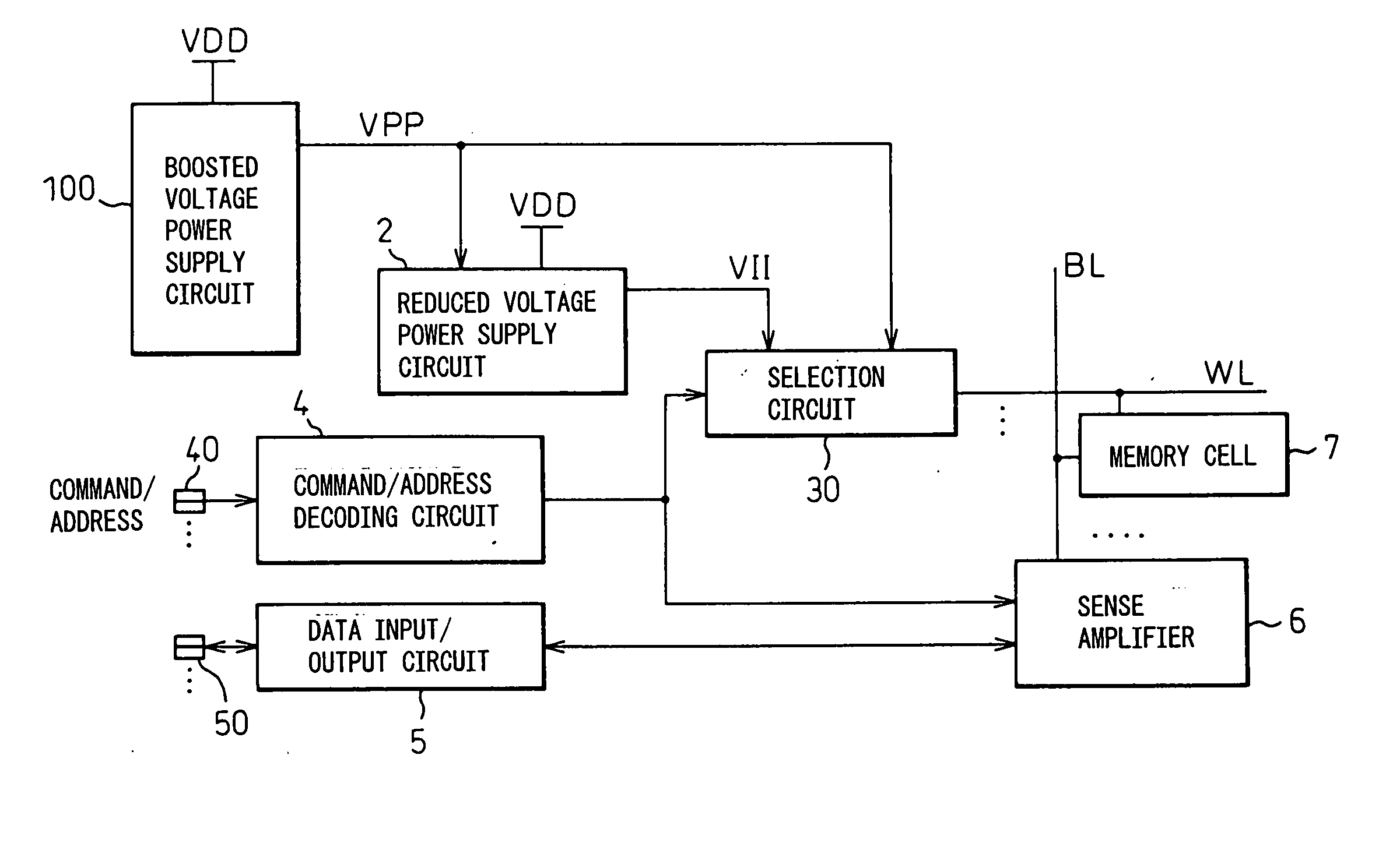
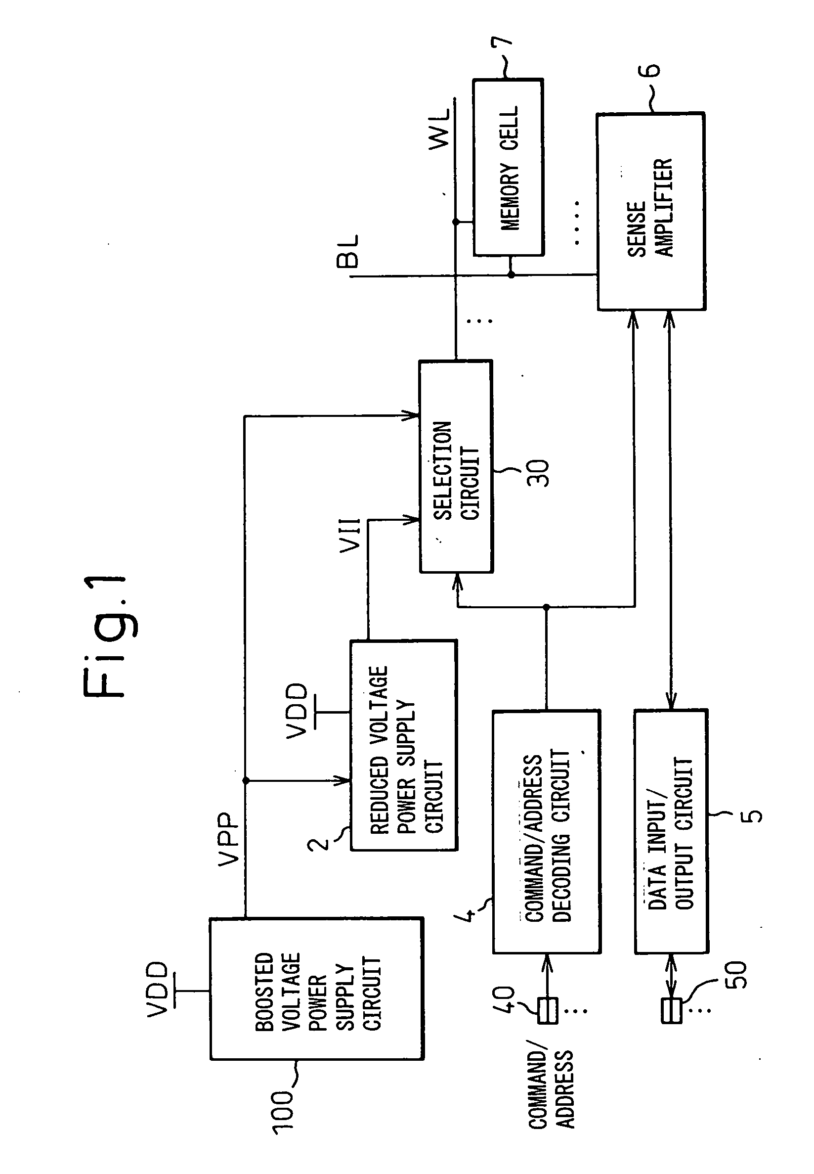
[0058]FIG. 9 is a circuit diagram showing a configuration of a main part of a boosted-voltage power-supply circuit in a semiconductor integrated circuit device according to the present invention, and FIG. 10 is a schematic waveform chart for describing operations of the boosted-voltage power-supply circuit of FIG. 9. Though a case in which the boosted-voltage power-supply circuit 1 boosts the high potential power supply voltage twice (VDD×2) will be described hereinafter, it is of course to be understood that the present invention may also be applied similarly to cases in which the high-potential power-supply voltage is boosted differently and is, for example, tripled (VDD×3).

[0059] As shown in FIG. 9, the boosted-voltage power-supply circuit 1 of this first embodiment comprises switches 10, 11, 12 and capacitances 15, 16, 17. As shown in FIGS. 9 and 10, first, in the state in which the switch 10 is turned on and the switches 11 and 12 are turned off, a node n1 is precharged from a ...

second embodiment

[0063]FIG. 11 is a circuit diagram showing a configuration of a main part of a boosted-voltage power-supply circuit in a semiconductor integrated circuit device according to the present invention.

[0064] As apparent from FIG. 11, in the boosted-voltage power-supply circuit in the semiconductor integrated circuit device of this second embodiment, a first diode 18 is provided in series with the first switch 11 in the forward direction and a second diode 19 is provided in series with the second switch 12 in the forward direction. As a result, for example, when the first output terminal OT1 and the second output terminal OT2 are short-circuited after the operation for activating the semiconductor integrated circuit device is completed, a backflow of current can be prevented and the boosted voltages VPP (VPP1, VPP2) can be generated efficiently.

third embodiment

[0065]FIG. 12 is a circuit diagram showing a configuration of a main part of a boosted-voltage power-supply circuit in a semiconductor integrated circuit device according to the present invention.

[0066] As apparent from a comparison between FIG. 12 and FIG. 11, in the boosted-voltage power-supply circuit in the semiconductor integrated circuit device of this third embodiment, only the second switch 12 is provided with the second diode 19. Here, the boosted-voltage power-supply circuit may be designed so that only the first switch 11 is provided with the first diode 18.


PUM


Abstract

A semiconductor integrated circuit device has a boosted-voltage power-supply circuit generating a boosted voltage, an internal circuit being driven with the boosted voltage, and a control circuit controlling the internal circuit by receiving the boosted voltage. The boosted-voltage power-supply circuit has a first output terminal for the internal circuit, and a second output terminal for the control circuit. The boosted voltage output from the second terminal has a specified level regardless of variation in the boosted voltage being output from the first terminal.

Description

CROSS-REFERENCE TO RELATED APPLICATION [0001] This application is a continuation application and is based upon PCT / JP03 / 05961, filed on May 13, 2003. BACKGROUND OF THE INVENTION [0002] 1. Field of the Invention [0003] The present invention relates to a semiconductor integrated circuit device and, in particular, it relates to a semiconductor integrated circuit device that uses an output voltage boosted by a boosted-voltage power-supply circuit for an internal circuit and to a control circuit that controls the internal circuit. [0004] 2. Description of the Related Art [0005] In recent years, semiconductor integrated circuit devices have been mounted on various portable apparatuses and their power supply voltage has been reduced. In the semiconductor integrated circuit devices driven by a low voltage, boosted-voltage power-supply circuits are used so that the semiconductor integrated circuit devices are operated by output voltages boosted by the boosted-voltage power-supply circuits. [...

Claims


Application Information

Patent Timeline
IPC IPC(8): G11C8/00G11C11/4074G11C11/408H02M3/07
CPCG11C5/14G11C5/145G11C8/08H02M2001/009G11C11/4074G11C11/4085H02M3/07G11C11/4072H02M1/009
Inventor YAMAZAKI, MASAFUMIUCHIDA, TOSHIYA
Owner SOCIONEXT INC
Why Eureka
Try Eureka