Display Device Driving Circuit and Display Device Including Same

a display device and driving circuit technology, applied in the direction of instruments, static indicating devices, etc., can solve the problems of display quality deterioration display quality deterioration, etc., to reduce the size of the display device driving circuit, reduce the amount of space occupied by the frame, and wide display area

Active Publication Date: 2008-07-03
SHARP KK
View PDF8 Cites 12 Cited by
  • Summary
  • Abstract
  • Description
  • Claims
  • Application Information

AI Technical Summary

Benefits of technology

[0032]According to the foregoing arrangement, the size of a display device driving circuit can be reduced. Therefore, a display device having a wide display area can be realized by reducing the amount of space that a frame occupies in a display section, i.e., the amount of space that a non-display region occupies in a display section.

Problems solved by technology

This causes such a problem that display quality deteriorates, for example, due to a decrease in display uniformity.
Such oscillations of the video signal causes display quality to deteriorate, for example, due to a decrease in display uniformity.
Furthermore, in addition to the increase in the amount of space that a dummy stage occupies, there is an increase in the amount of space in which wires are provided.
This causes an increase in the amount of space for a frame surrounding a display area.
Therefore, the respective techniques of Tokukaihei 7-295520 and Tokukai 2004-54235 are not suitable for a display device, such as a display device to be provided in a portable phone or the like, which is required to be small and to have, for the purpose of miniaturization, a small amount of space for a frame surrounding a display area.
This causes an increase in the amount of space that the precharge signal switching circuit occupies and an increase in the amount of space in which wires are provided, thereby causing an increase in the size of the driving circuit.
Thus, the conventional display device driving circuit has such a problem that the amount of space that the driving circuit occupies and the amount of space in which wires are provided are increased for the purpose of performing precharge.

Method used


Image

  • Display Device Driving Circuit and Display Device Including Same
  • Display Device Driving Circuit and Display Device Including Same
  • Display Device Driving Circuit and Display Device Including Same

Examples


embodiment 1

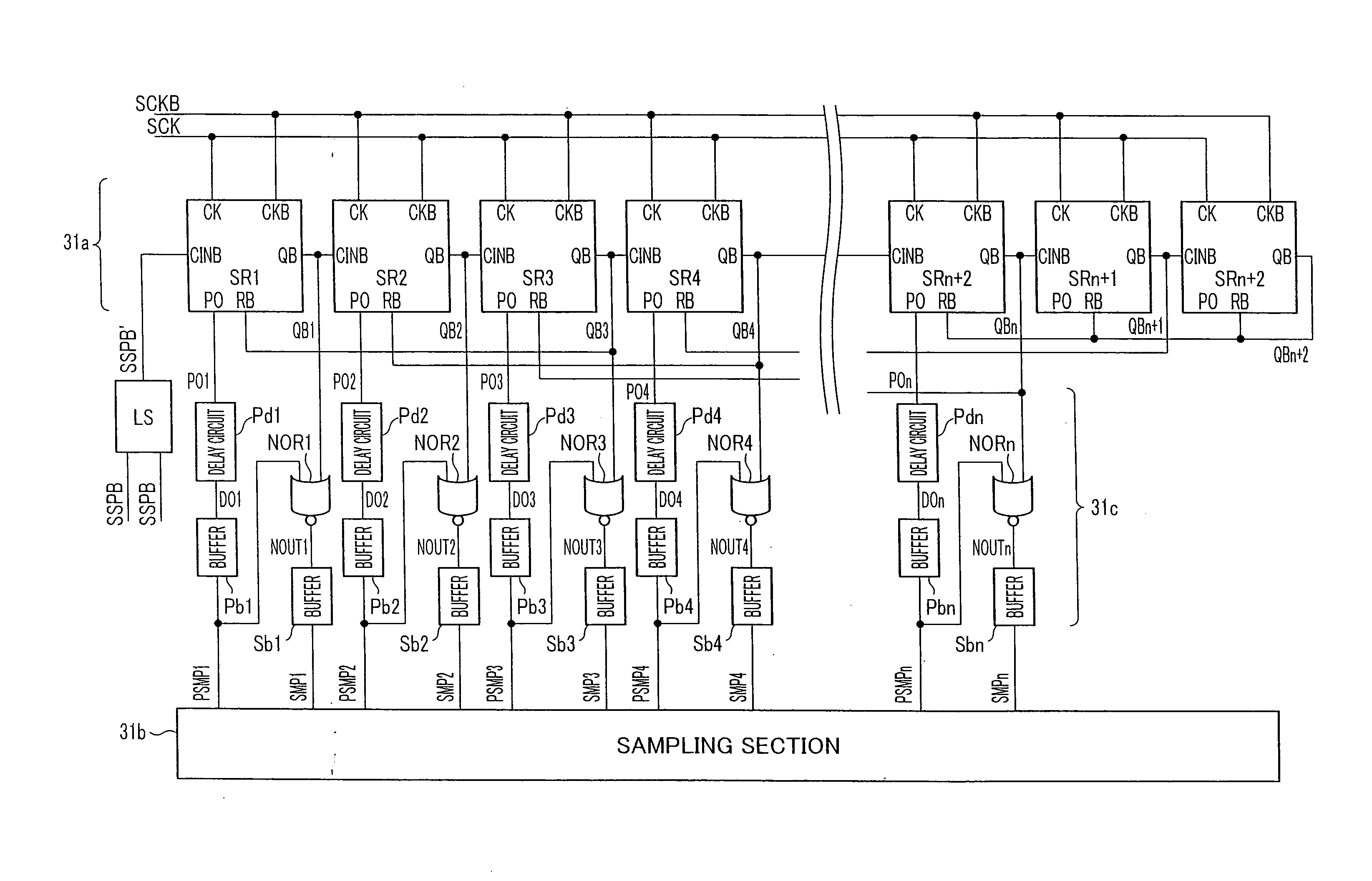
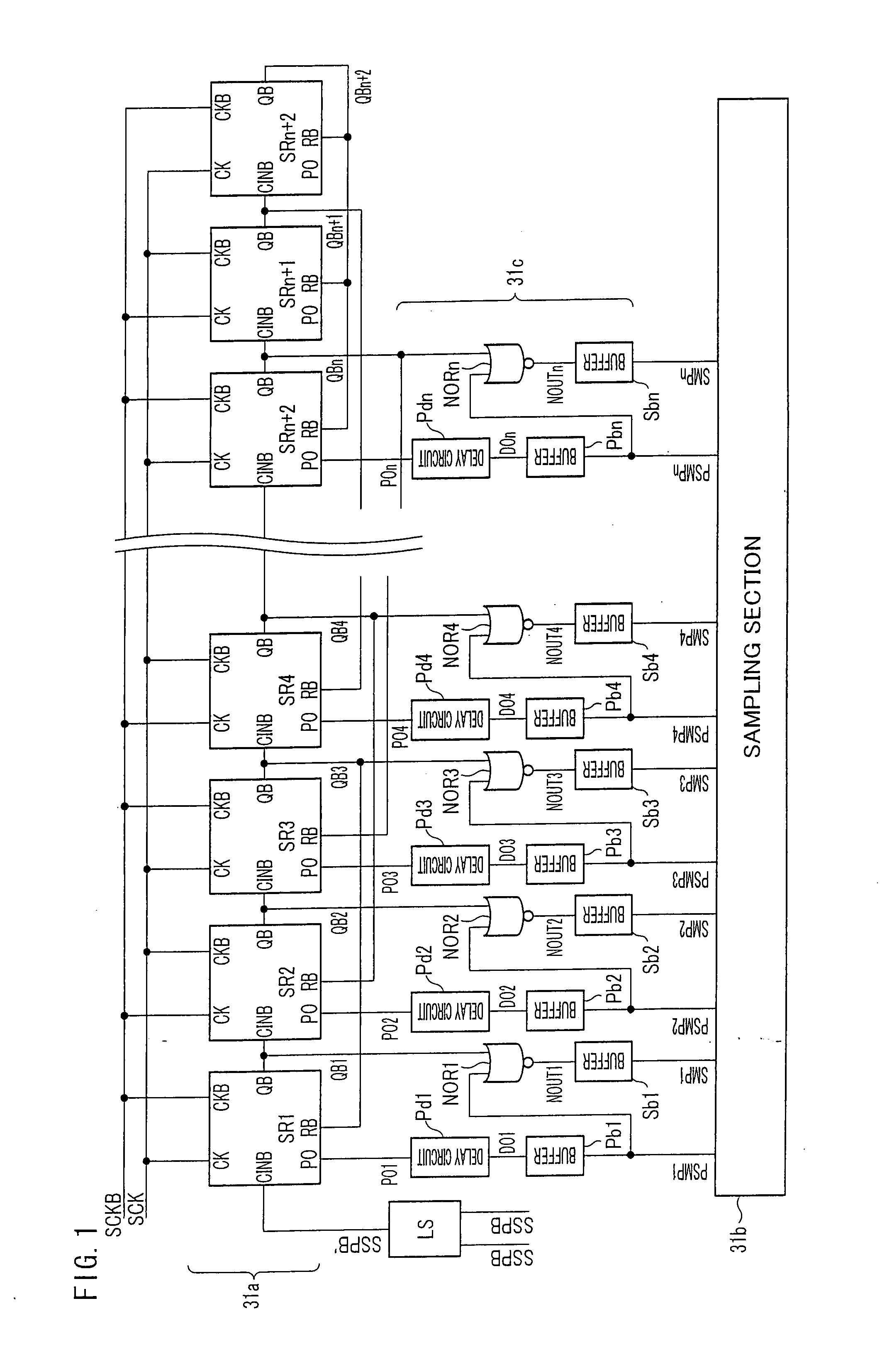
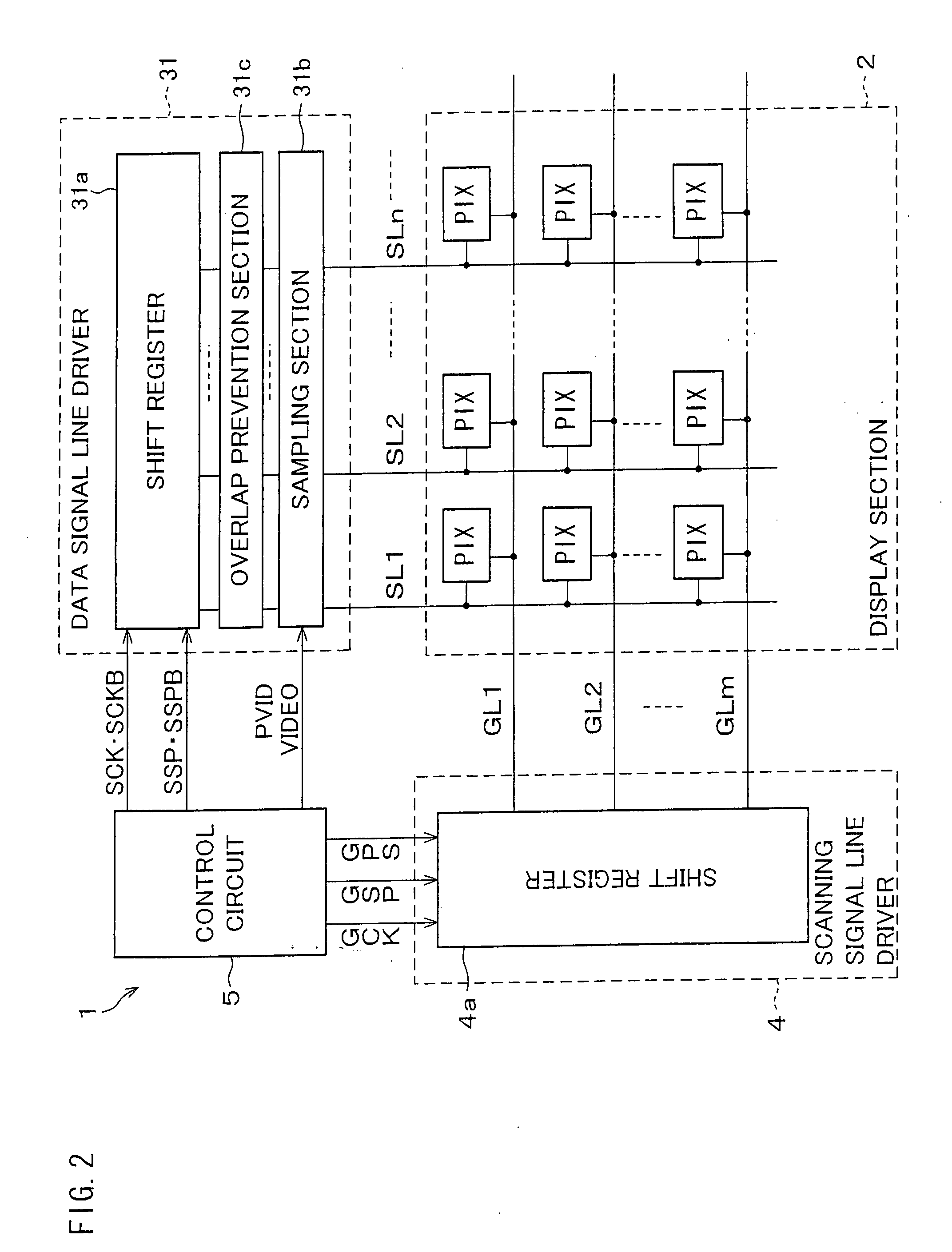
[0068]An embodiment of the present invention is described with reference to the drawings. FIG. 1 is a block diagram showing a structure of a data signal line driver 31, which is a display device driving circuit according to the present embodiment. As shown in FIG. 2, the data signal line driver 31 is a data signal line driver for driving data signal lines SL1, SL2, . . . of a liquid crystal display device (display device) 1.

[0069](Liquid Crystal Display Device 1)

[0070]The liquid crystal display device 1 is an active-matrix liquid crystal display device in which pixels are driven in a dot-sequential manner and by alternating current. The liquid crystal display device 1 includes a display section 2 having pixels PIX arrayed in a matrix manner, a data signal line driver 31 and a scanning signal line driver 4 both driving each of the pixels PIX, a control circuit 5, data signal lines SL1, SL2, . . . , and scanning signal lines GL1, GL2, . . . . Moreover, the control circuit 5 generates ...

modified example 1

of the Flip-Flop SR

[0208]In the present embodiment, the shift register 31a includes a plurality of set-reset flip-flops. However, the present invention is not limited to this.

[0209]For example, the flip-flops SR (SR1, SR2, . . . , SRn+2) may be respectively replaced by shift register blocks SRB (SRB1, SRB2, . . . , SRBn+2) each including a gating circuit and a flip-flop each described in Patent Document 8. In FIG. 18, the arrangement of the flip-flop in Patent Document 8 is changed for the sake of convenience.

[0210]As shown in FIG. 18, each of the shift register blocks SRB includes a control circuit CN, a gating circuit GC, a flip-flop F, and an inverter I50. Further, as with each of the flip-flops SR, each of the shift register blocks SRB includes a CK terminal, a CKB terminal, a CINB terminal, an RB terminal, a PO terminal, and a QB terminal. Moreover, the same signals as with the flip-flop SR are inputted to and outputted from the terminals, respectively.

[0211]The control circuit...

modified example 2

of the Flip-Flop SR

[0233]Further, the flip-flop SR (SR1, SR2, . . . , SRn+2) shown in FIG. 4 may be replaced by a flip-flop SR_100 (SR_1001, SR_1002, . . . , SR_100n+2) shown in FIG. 32. FIG. 32 is a block diagram showing a structure of each flip-flop SR_100. As shown in FIG. 32, the flip-flop SR includes a level shifter control circuit CN_100, a level shifter LS_100, a set-reset flip-flop SR-FF, an inverter I1, an inverter I2, and an inverter I3. Note that the flip-flop SR-FF is arranged in the same manner as in FIG. 4.

[0234](Level Shifter Control Circuit CN_100)

[0235]FIG. 33 is a block diagram showing a structure of the level shifter control circuit (control circuit) CN_100. As shown in FIG. 33, the level shifter control circuit CN_100 includes two input terminals IN1 and IN2, an inverter ICN, a switch SWCN, a P-channel MOS transistor (TFT) PCN2, and an output terminal CNOUTB. Note that the switch SWCN is an analog switch including an N-channel MOS transistor (TFT) NCN and a P-cha...


PUM


Abstract

In an embodiment, a sampling signal to each data signal line is generated by using an output signal outputted from each flip-flop, and a precharge signal by which the data signal line to which the sampling signal is to be outputted is precharged is generated by using an output signal outputted from an output terminal of the flip-flop. Further, by providing a NOR circuit, an active period of the precharge signal and an active period of the sampling signal are prevented from overlapping each other. With this, in an embodiment of a display device driving circuit, including a precharge circuit, which causes a precharge power supply to precharge signal supply lines, the number of shift registers and the size of a circuit can be reduced.

Description

TECHNICAL FIELD[0001]The present invention relates to (i) a driving circuit for supplying a write signal to signal supply lines of a display device after having precharged the signal supply lines and (ii) a display device including the driving circuit.BACKGROUND ART[0002]In driving a liquid crystal panel of a dot-sequential active-matrix liquid crystal display device by alternating current, before a video signal is supplied to pixels via data signal lines, each of the data signal lines is precharged. With this, each of the pixels is stably charged so as to have a desired quantity of electric charge. In this case, because the total wiring capacitance of the data signal lines is high, an attempt to precharge all the data signal lines at once requires a precharge power supply having high driving capability. This problem can be solved by a technique for precharging each unit of a small number of data signal lines.[0003]For example, Japanese Unexamined Patent Application No. 295520 / 1995 ...

Claims


Application Information

Patent Timeline
Patent Type & Authority Applications(United States)
IPC IPC(8): G09G3/36
CPCG09G2310/0248G09G3/3688
Inventor MURAKAMI, YUHICHIROHWASHIO, HAJIME
Owner SHARP KK
Why Eureka
Try Eureka