
Source plate for liquid crystal displays, and liquid crystal display device having source plate

a liquid crystal display and source plate technology, applied in non-linear optics, instruments, optics, etc., can solve the problems of increasing production costs and fabrication expenses, and achieve the effect of reducing the amount of liquid crystal wasted during manufacturing

Active Publication Date: 2008-07-03
SAMSUNG DISPLAY CO LTD
View PDF4 Cites 0 Cited by
  • Summary
  • Abstract
  • Description
  • Claims
  • Application Information

AI Technical Summary

Benefits of technology

[0014]An aspect of the present invention is to provide a liquid crystal display source plate capable of reducing the amount of liquid crystal wasted during manufacturing.
[0015]Another aspect of the present invention is to provide a liquid crystal display that is less expensive to fabricate.
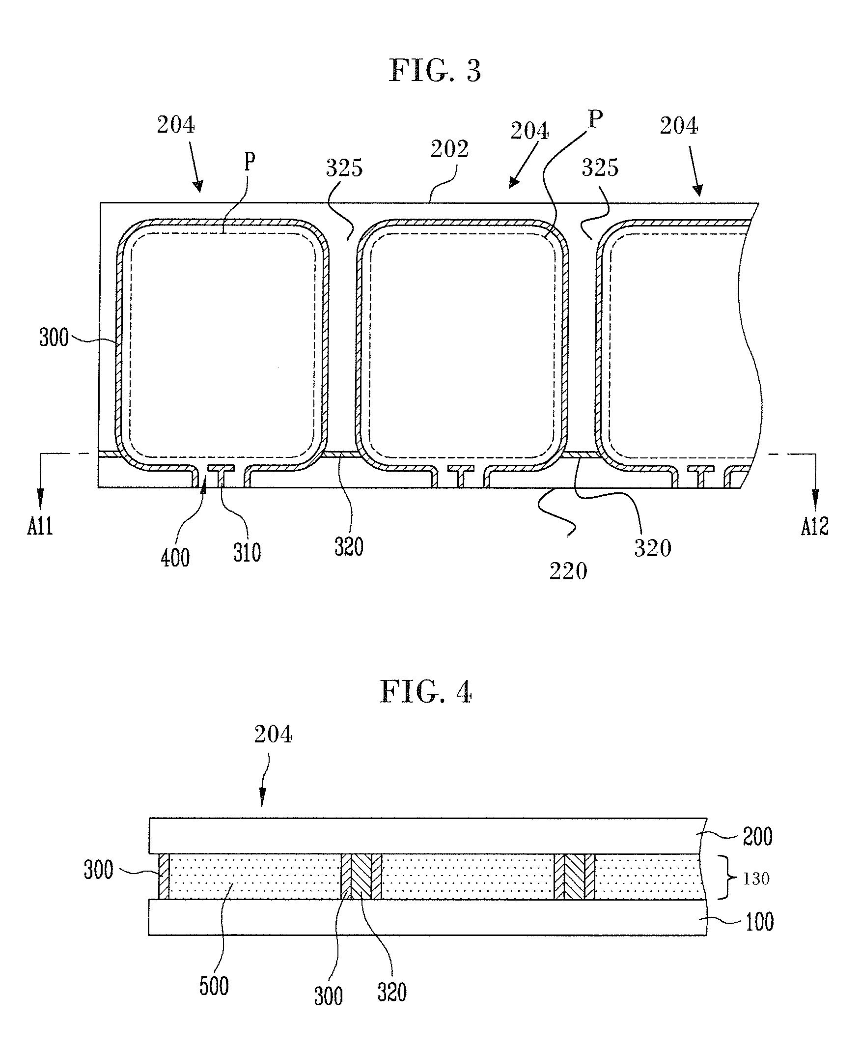
[0016]A source plate, according to the above and / or other aspects of the present invention, includes a first substrate, including first electrodes disposed on a plurality of pixel regions thereof; a second substrate disposed in opposition to the first substrate, including second electrodes disposed on a plurality of pixel regions thereof; sealing agents surrounding each pixel region, and are positioned between the first substrate and the second substrate; gaps in the sealing agents form liquid crystal inlets; and assistance sealing agents positioned between adjacent sealing agents. Liquid crystal is injected between the first substrate and the second substrate, through the liquid crystal inlets. The assistance sealing agents prevent the liquid crystal from entering the space between the sealing agents.

Problems solved by technology

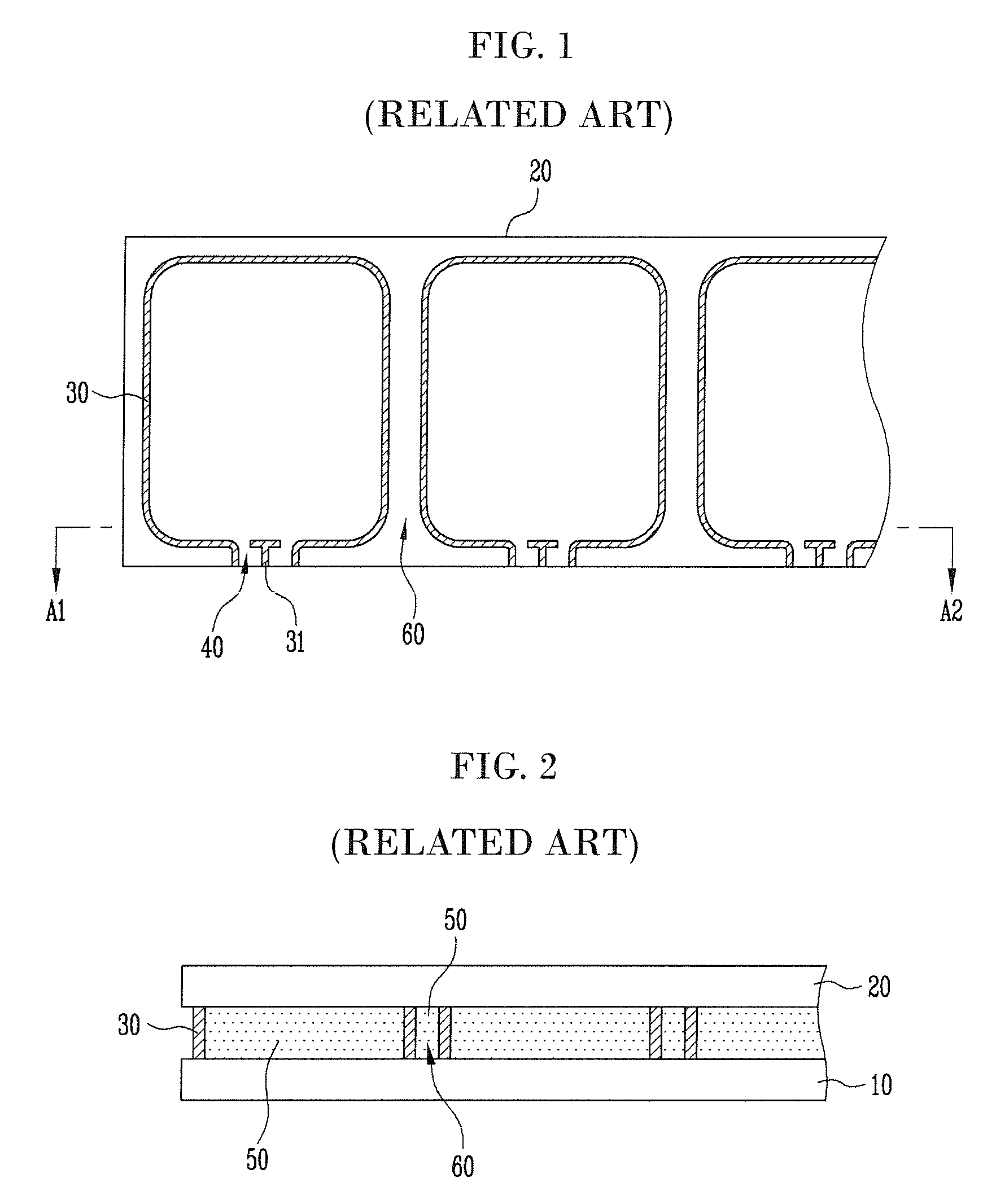
Accordingly, the liquid crystal 50 that flows into the space 60 is wasted, thus increasing production costs and fabrication expenses.

Method used


Image

  • Source plate for liquid crystal displays, and liquid crystal display device having source plate
  • Source plate for liquid crystal displays, and liquid crystal display device having source plate
  • Source plate for liquid crystal displays, and liquid crystal display device having source plate

Examples


Embodiment Construction

[0024]Reference will now be made in detail to the present embodiments of the present invention, examples of which are illustrated in the accompanying drawings, wherein like reference numerals refer to the like elements throughout. The embodiments are described below in order to explain the present invention by referring to the Figures.

[0025]FIG. 3 is a plane view of a source plate, according to an embodiment of the present invention, and illustrates a part of a substrate of an array-type liquid crystal display. FIG. 4 illustrates a cross sectional view take along the line A11-A12 of FIG. 3.

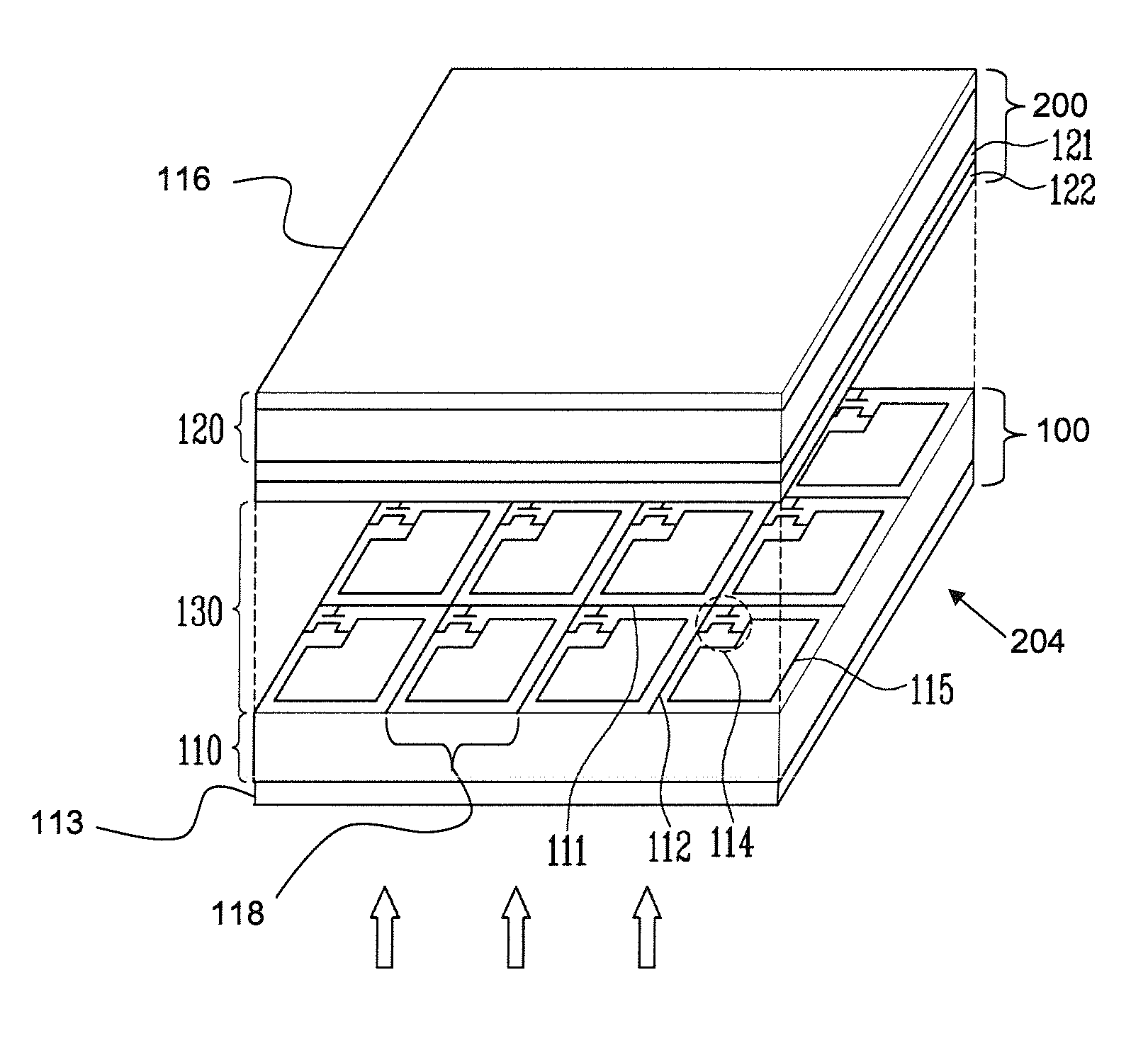
[0026]Referring to FIG. 3 and FIG. 4, a source plate 202 comprises a plurality of liquid crystal displays 204. Each liquid crystal display 204 includes: a lower substrate 100, including pixel electrodes, disposed in a pixels regions P; an upper substrate 200 disposed opposite the lower substrate 100, including one or more transparent electrodes disposed in the pixel regions P; a plurality of seali...


PUM


Abstract

A source plate for a liquid crystal display, a fabrication method thereof, and a liquid crystal display produced by the method. The source plate includes a first substrate, including a plurality of pixel regions having first electrodes respectively disposed therein; a second substrate, including a plurality of pixel regions having second electrodes disposed therein, positioned to be in opposition to the first substrate; a sealing agent surrounding each pixel region, disposed between the first substrate and the second substrate; a liquid crystal inlet disposed at an opening in each of the sealing agents; an assistance sealing agent disposed between adjacent sealing agents; and a liquid crystal disposed in the pixel regions. The method includes forming the assistance sealing agents to prevent injected liquid crystal from entering a space between the pixel regions.

Description

CROSS-REFERENCE TO RELATED APPLICATION[0001]This application claims the benefit of Korean Application No. 2007-369, filed Jan. 2, 2007, in the Korean Intellectual Property Office, the disclosure of which is incorporated herein by reference.BACKGROUND OF THE INVENTION[0002]1. Field of the Invention[0003]Aspects of the present invention relate to a source plate for a liquid crystal display a method for fabricating a liquid crystal display.[0004]2. Description of the Related Art[0005]There has been an increasing demand for display devices due to the growth of the information and communications industries. Recently, there has been an increase in the demand for high resolution displays that are small, light weight, thin, and have low power requirements. In order to satisfy this demand, liquid crystal displays that use organic light emitters have been developed.[0006]One of the most widely used type of flat panel displays is a thin film transistorliquid crystal display (TFT-LCD). TFT-LCD...

Claims


Application Information

Patent Timeline
IPC IPC(8): G02F1/1339
CPCG02F1/1341G02F1/1339
Inventor LEE, HAK SUNG
Owner SAMSUNG DISPLAY CO LTD
Learn More