Supercharge Your Innovation With Domain-Expert AI Agents!

By-die-exposure for patterning of holes in edge die

a technology of edge die and patterning hole, which is applied in the direction of liquid surface applicators, coatings, instruments, etc., can solve the problems of small dimension, difficult patterning of wafer edge dies, and deformation of features near the rounded edge of the wafer

Active Publication Date: 2008-07-03
TEXAS INSTR INC
View PDF5 Cites 7 Cited by
  • Summary
  • Abstract
  • Description
  • Claims
  • Application Information

AI Technical Summary

Benefits of technology

[0005]In accordance with the invention, there is a method of making a semiconductor device. The method can include forming a photoresist layer over a surface of a wafer, wherein the wafer includes an edge that has a substantially rounded profile, an array of dies, and at least one edge die. The method can also include dividing a shot area into a plurality of shot portions and assigning a blind ID to each of the plurality of shot portions. The method can further include identifying one or more edge shot portions on the edge of the wafer for additional exposure; and exposing one or more times identified one or more edge shot portions on the edge of the wafer and blocking non-identified one or more non-edge shot portions.

Problems solved by technology

This standard exposure intensity, however, can result in deformities in the features formed near the rounded edge of the wafer, especially on partial edge shots.
In particular, via holes with small dimension and high aspect ratio are difficult to pattern on the wafer edge dies due to wafer edge topography.
However it does not permit localized exposure adjustment on dies within a shot.
Although theoretically all dies can be exposed with different, optimized exposures, compromised scanner throughput makes this impractical.

Method used


Image

  • By-die-exposure for patterning of holes in edge die
  • By-die-exposure for patterning of holes in edge die
  • By-die-exposure for patterning of holes in edge die

Examples


Embodiment Construction

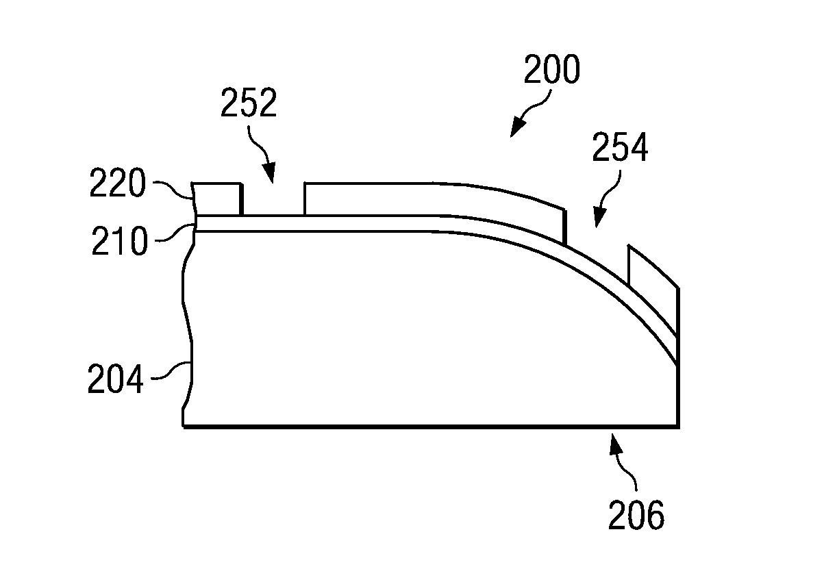
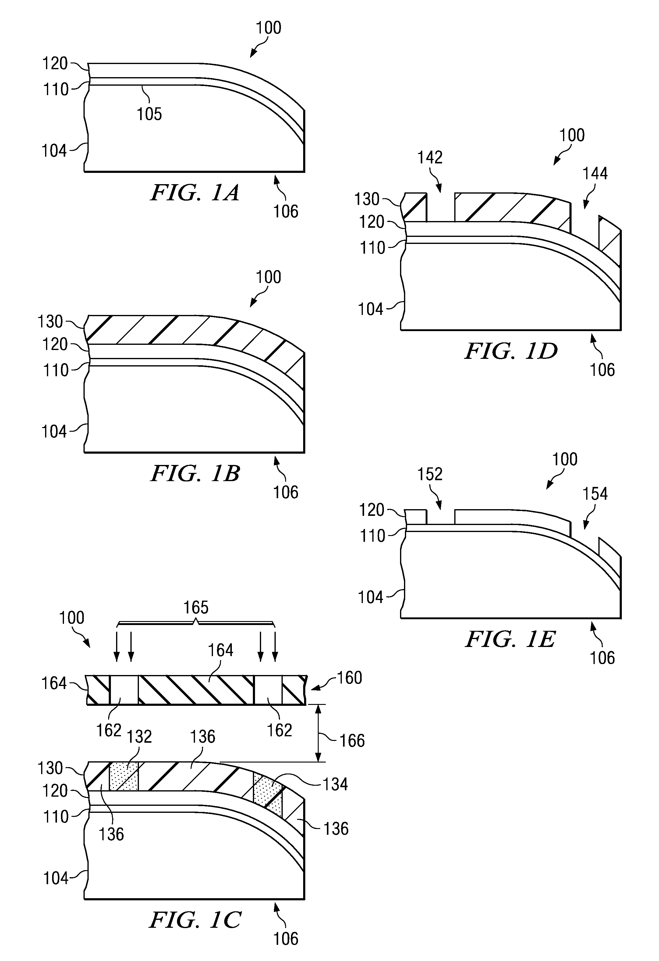
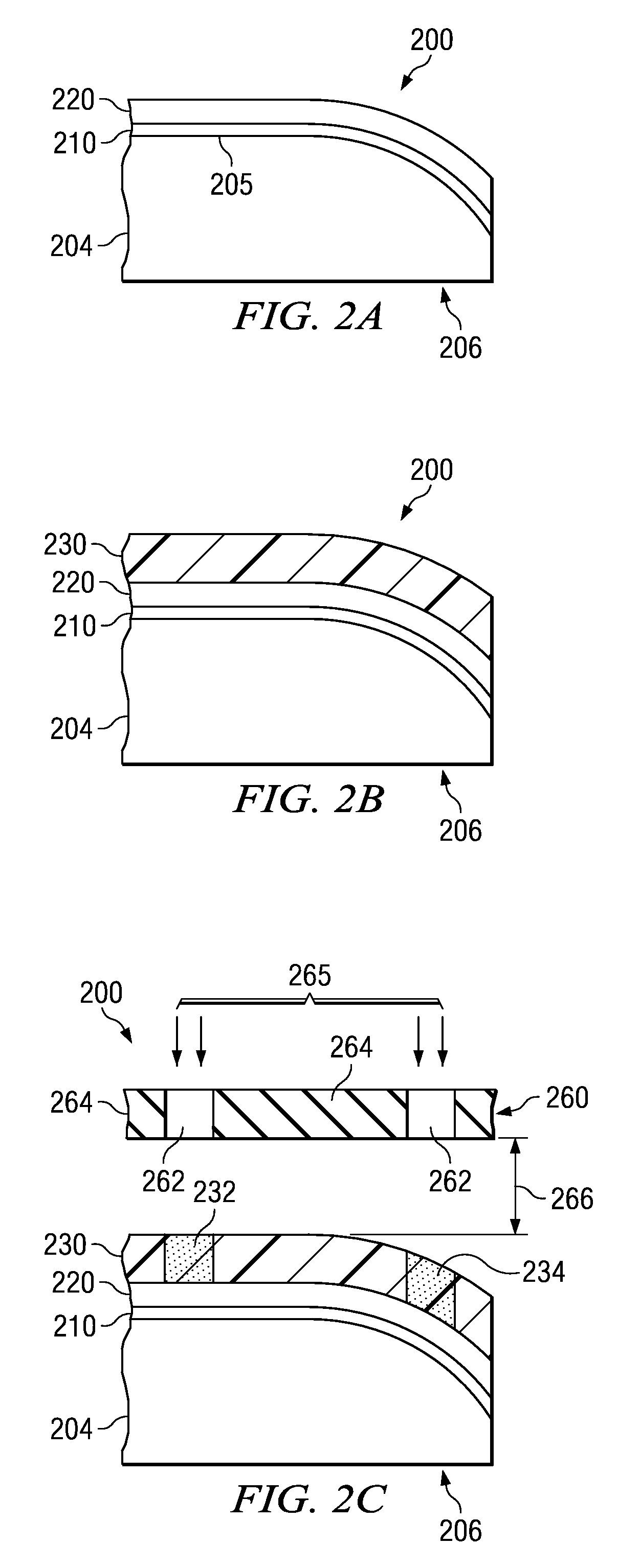
[0016]Reference will now be made in detail to the present embodiments, examples of which are illustrated in the accompanying drawings. Wherever possible, the same reference numbers will be used throughout the drawings to refer to the same or like parts.

[0017]Notwithstanding that the numerical ranges and parameters setting forth the broad scope of the invention are approximations, the numerical values set forth in the specific examples are reported as precisely as possible. Any numerical value, however, inherently contains certain errors necessarily resulting from the standard deviation found in their respective testing measurements. Moreover, all ranges disclosed herein are to be understood to encompass any and all sub-ranges subsumed therein. For example, a range of “less than 10” can include any and all sub-ranges between (and including) the minimum value of zero and the maximum value of 10, that is, any and all sub-ranges having a minimum value of equal to or greater than zero an...


PUM


Abstract

In accordance with the invention, there are semiconductor devices and methods of making semiconductor devices and holes. The method of making a semiconductor device can comprise forming a photoresist layer over a surface of a wafer, wherein the wafer comprises an edge that has a substantially rounded profile, an array of dies, and at least one edge die. The method can also comprise dividing a shot area into a plurality of shot portions and assigning a blind ID to each of the plurality of shot portions. The method can further comprise identifying one or more edge shot portions on the edge of the wafer for additional exposure; and exposing one or more times identified one or more edge shot portions on the edge of the wafer and blocking non-identified one or more non-edge shot portions.

Description

FIELD OF THE INVENTION [0001]The subject matter of this invention relates to fabricating a semiconductor device. More particularly, the subject matter of this invention relates to a system and method for the exposure of edge dies.BACKGROUND OF THE INVENTION [0002]Conventional semiconductor fabrication utilizes a scanner or other light source to form devices or features on the surface of a wafer. More specifically, a beam of light is directed at a portion of the wafer through a mask to cover a spatial area called the “shot” area. The shot area generally covers a group of dies on the wafer or a single die depending on the size of the die and the configuration of the mask. For the case of multiple dies within a shot, the shot area covers an array of die—for example, three die in one direction and two die in the perpendicular direction. This configuration is referred to as a ‘full shot.’ At the edge of the wafer where the full die or full shot pattern is not present, the shot area consi...

Claims


Application Information

Patent Timeline
Patent Type & Authority Applications(United States)
IPC IPC(8): H01L21/469
CPCG03F7/70425H01L21/76816G03F7/70625
Inventor DETWEILER, SHANGTINGCHATTERJEE, BASABATKINSON, CHRIS D.GULDI, RICHARD L.
Owner TEXAS INSTR INC
Features
  • R&D
  • Intellectual Property
  • Life Sciences
  • Materials
  • Tech Scout
  • Unparalleled Data Quality
  • Higher Quality Content
  • 60% Fewer Hallucinations
Learn More