

High-frequency circuit, high-frequency device, and communication apparatus
Inactive Publication Date: 2008-07-10
HITACHI METALS LTD
View PDF13 Cites 42 Cited by
- Summary
- Abstract
- Description
- Claims
- Application Information
AI Technical Summary
Benefits of technology
[0009]Accordingly, an object of the present invention is to provide a small high-frequency circuit having good receiving sensitivity, which can be used for dual-band wireless apparatuses.
Problems solved by technology
Accordingly, when a bandpass filter or a lowpass filter having insertion loss of about 2 dB is used, or when a diplexer circuit having insertion loss of about 1 dB is used on the input side of the low-noise amplifier, the receiving sensitivity is limited.
Though this circuit achieves the reduction of harmonics on the transmitting and receiving sides by one bandpass filter, it cannot be used in two frequency bands of a 2.4-GHz band and a 5-GHz band, and its receiving sensitivity is limited because it comprises a bandpass filter and a diplexer circuit on the input side of the low-noise amplifier.
However, the high-frequency circuits of WO2006 / 003959A and JP2002-208874A fail to satisfactorily handle IEEE802.11n.
Method used
View moreImage
Smart ImageViewing Examples

Examples
examples 3 and 4
[0131]In the high-frequency device of Example 3 comprising the high-frequency circuit shown in FIG. 1 having no variable notch filter circuit, a signal of −15 dBm in a 2.4-GHz band was inputted into the low-noise amplifier circuit, and a second harmonic of −30 dBm was output from the receiving terminal of a 5-GHz band. On the other hand, in the high-frequency device of Example 4 comprising the high-frequency circuit shown in FIG. 10 having a variable notch filter circuit, harmonics output from the receiving terminal of 5-GHz band were reduced to −70 dm, preventing the deterioration of receiving sensitivity,
Login to View More PUM
 Abstract
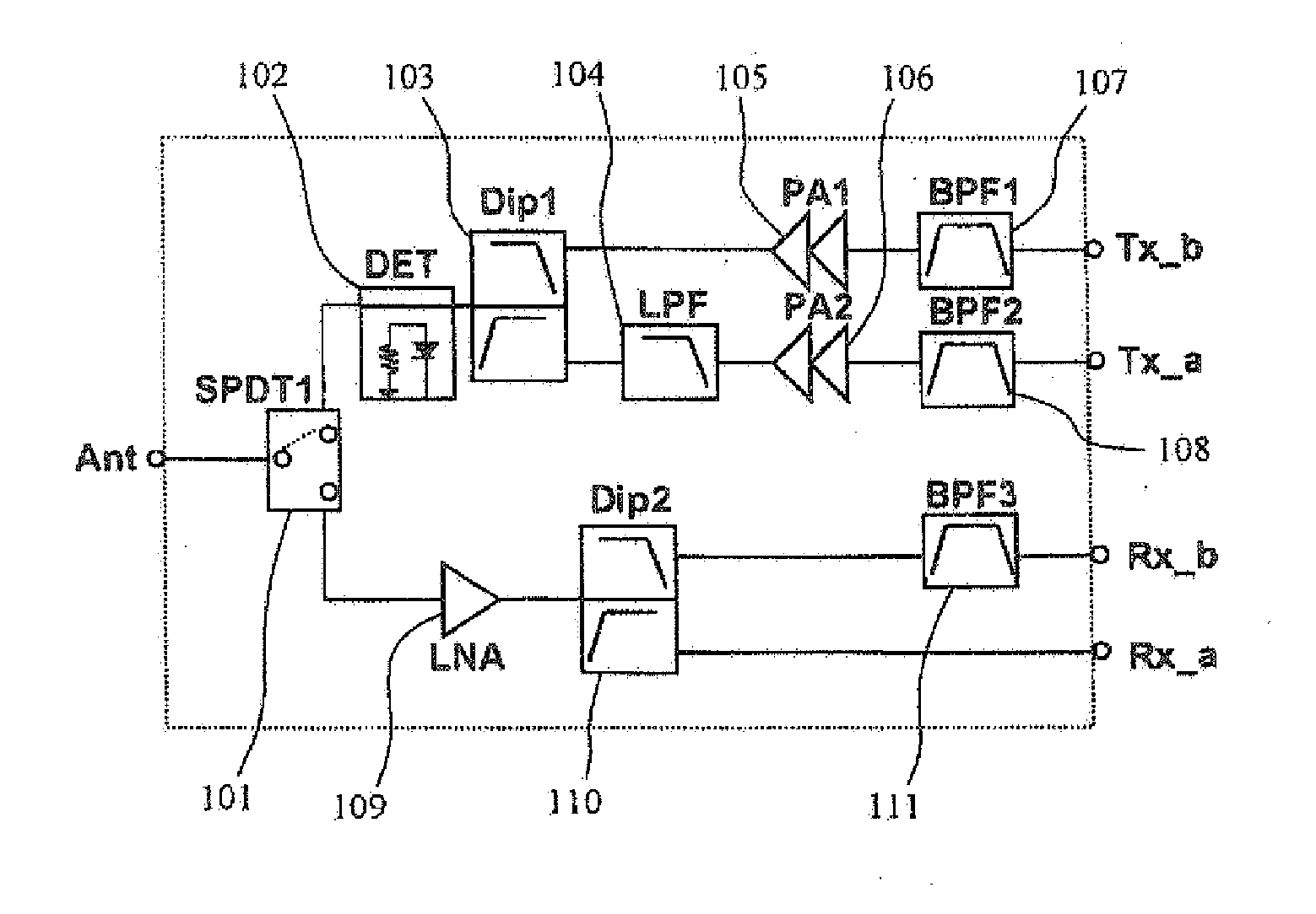
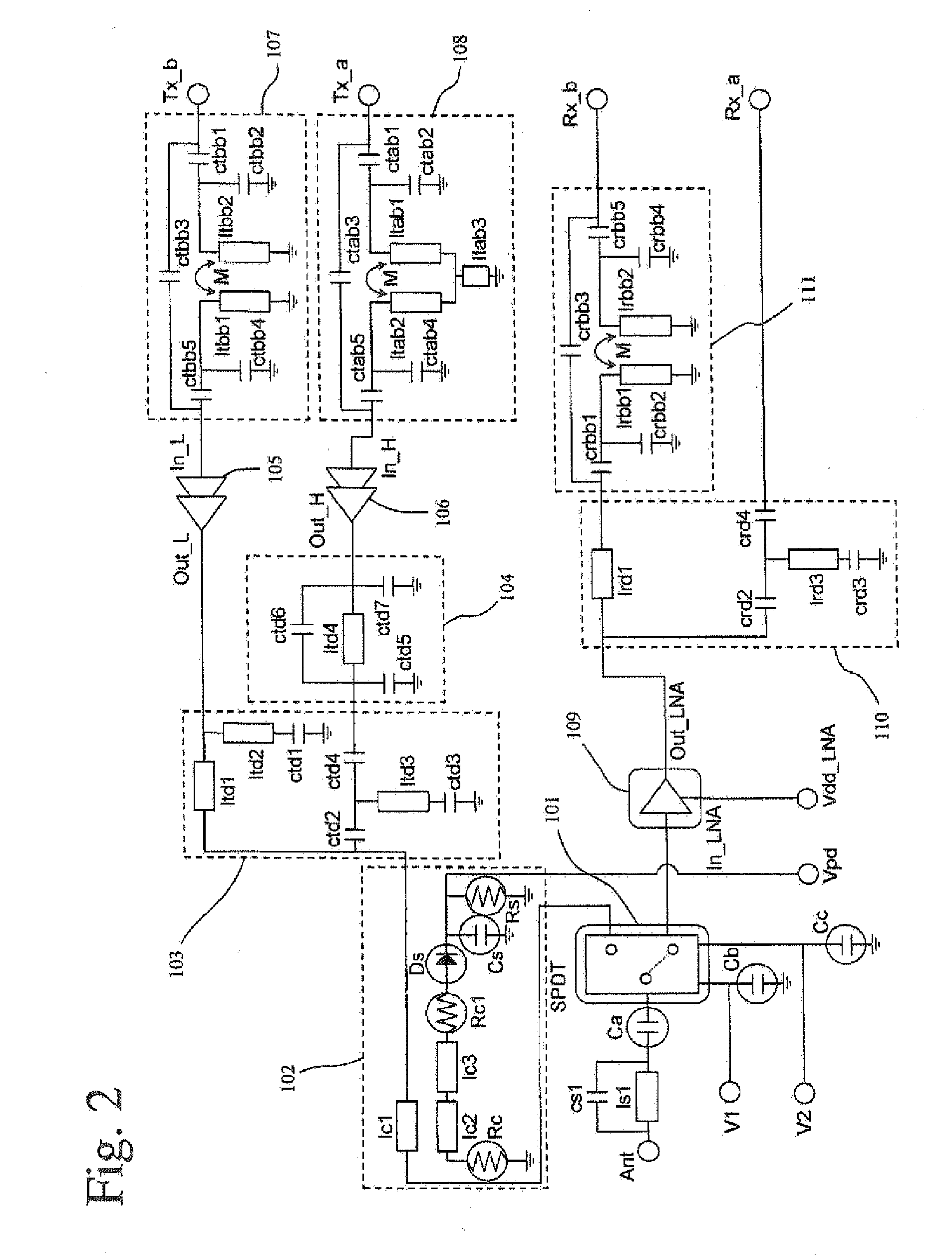
A high-frequency circuit comprising a switch circuit connected to an antenna terminal, first and second diplexer circuits connected to the switch circuit, first and second power amplifier circuits connected to the first diplexer circuit, first and second bandpass filter circuits connected to the first and second power amplifier circuits, a third bandpass filter circuit connected to the second diplexer circuit, a detection circuit disposed between the switch circuit and the first diplexer circuit, and a low-noise amplifier circuit disposed between the switch circuit and the second diplexer circuit.
Description
FIELD OF THE INVENTION[0001]The present invention relates to a high-frequency circuit adapted to at least two communications systems usable for wireless communications among electronic / electric apparatuses, and a high-frequency device comprising such a high-frequency circuit and a communications apparatus comprising it.BACKGROUND OF THE INVENTION[0002]Data communications by wireless LAN such as IEEE802.11 are now widely used, for instance, in personal computers (PCs), PC peripherals such as printers, hard disk drives and broadband rooters, electronic apparatuses such as FAXs, refrigerators, standard televisions (SDTVs), high-definition televisions (HDTVs), digital cameras, digital video cameras and mobile phones, signal-transmitting means in automobiles and aircrafts, etc.[0003]As the wireless LAN standard, IEEE802.11a uses an orthogonal frequency division multiples (OFDM) modulation system in a frequency band of 5 GHz, supporting high-speed data communications of maximum 54 Mbps. I...
Claims
Login to View More Application Information
Patent Timeline
 IPC IPC(8): H04B1/44
CPCH04B1/50H04B1/0057
InventorFUKAMACHI, KEISUKEKEMMOCHI, SHIGERUSATAKE, HIROTAKA
OwnerHITACHI METALS LTD