Delay locked loop circuits and method for controlling the same

Inactive Publication Date: 2008-07-17
SAMSUNG ELECTRONICS CO LTD
View PDF7 Cites 2 Cited by
  • Summary
  • Abstract
  • Description
  • Claims
  • Application Information

AI Technical Summary

Benefits of technology

[0021]An exemplary embodiment of the present invention provides a delay locked loop circuit and a method for controlling the same that are capable of preventing or minimizing logic failures.
[0022]An exemplary embodiment of the present invention provides a delay locked loop circuit

Problems solved by technology

Because the operational speed of the peripheral devices cannot keep pace with operation speed of microprocessors, however, there is always a speed difference between new microprocessors and their corresponding peripheral devices.
In this case, a logic failure may occur due to insufficient delay cells of the delay chain 10.
This phenomenon may occur when an operat

Method used


Image

  • Delay locked loop circuits and method for controlling the same
  • Delay locked loop circuits and method for controlling the same
  • Delay locked loop circuits and method for controlling the same

Examples


Example

[0040]Exemplary embodiments of the present invention will now be described more fully hereinafter with reference to the accompanying drawings, in which exemplary embodiments of the invention are shown. The present invention may, however, be embodied in different forms and should not be construed as limited to the exemplary embodiments set forth herein. Rather, these exemplary embodiments are provided as teaching examples of the present invention. Like numbers refer to like elements throughout the drawings.

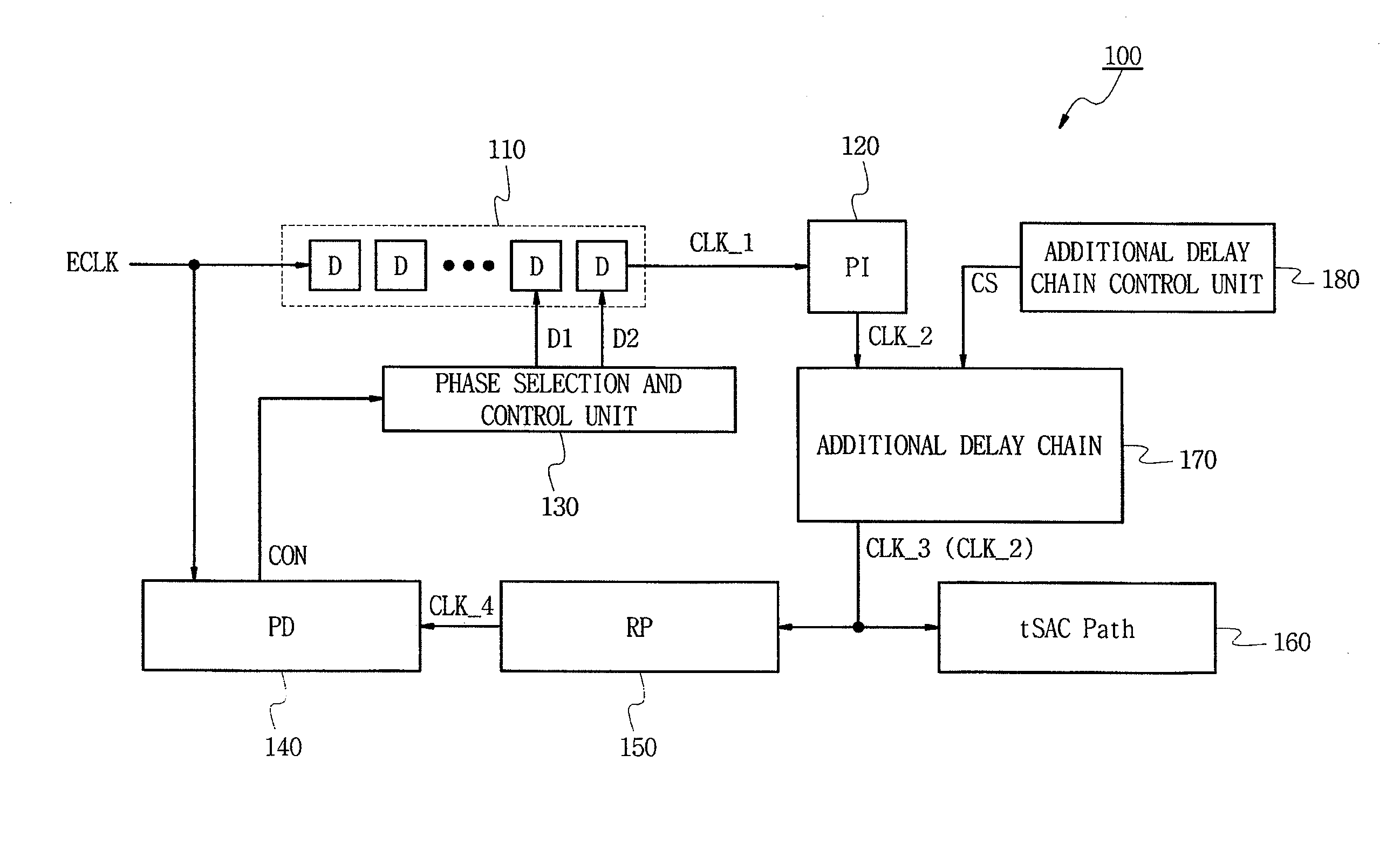
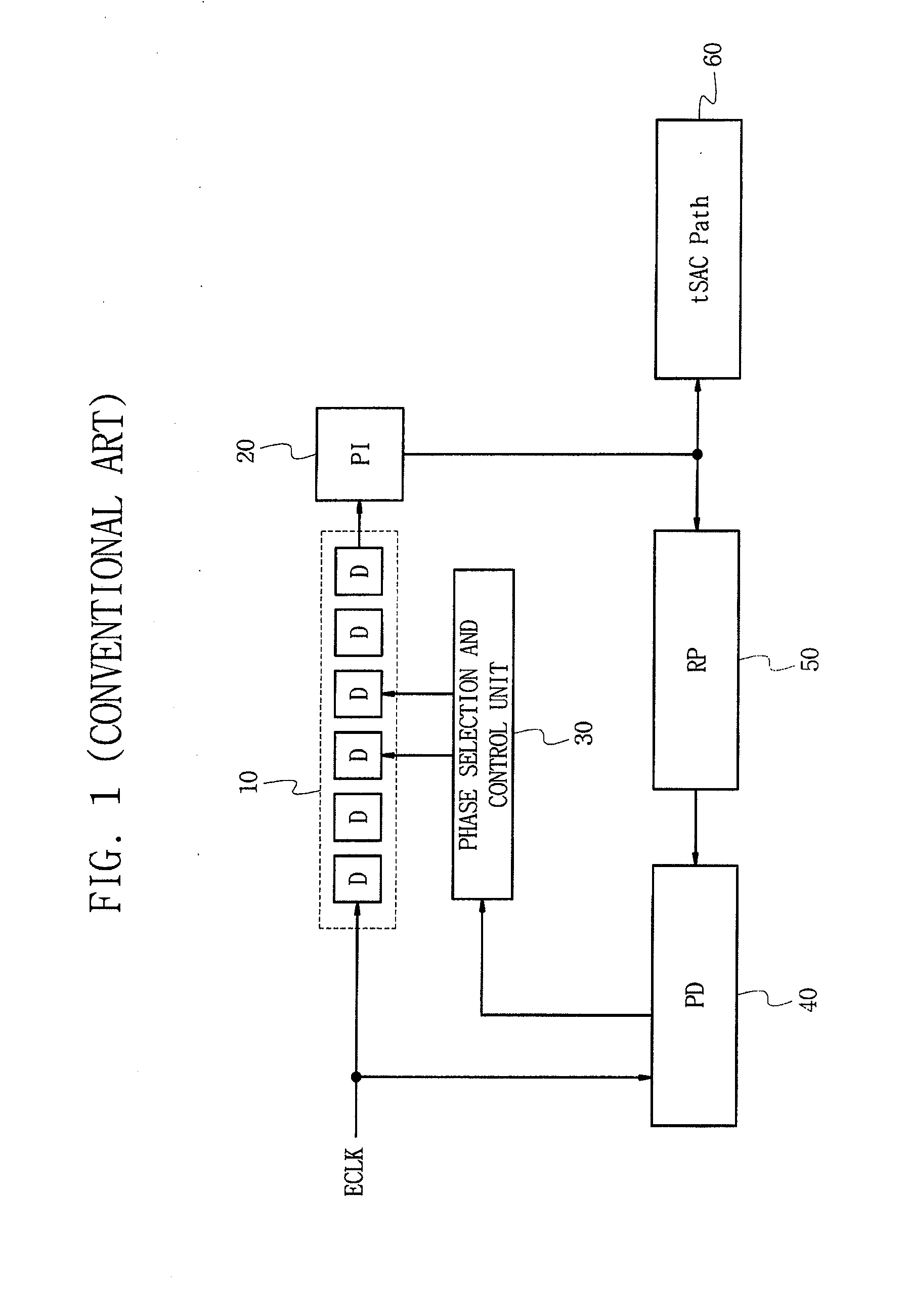
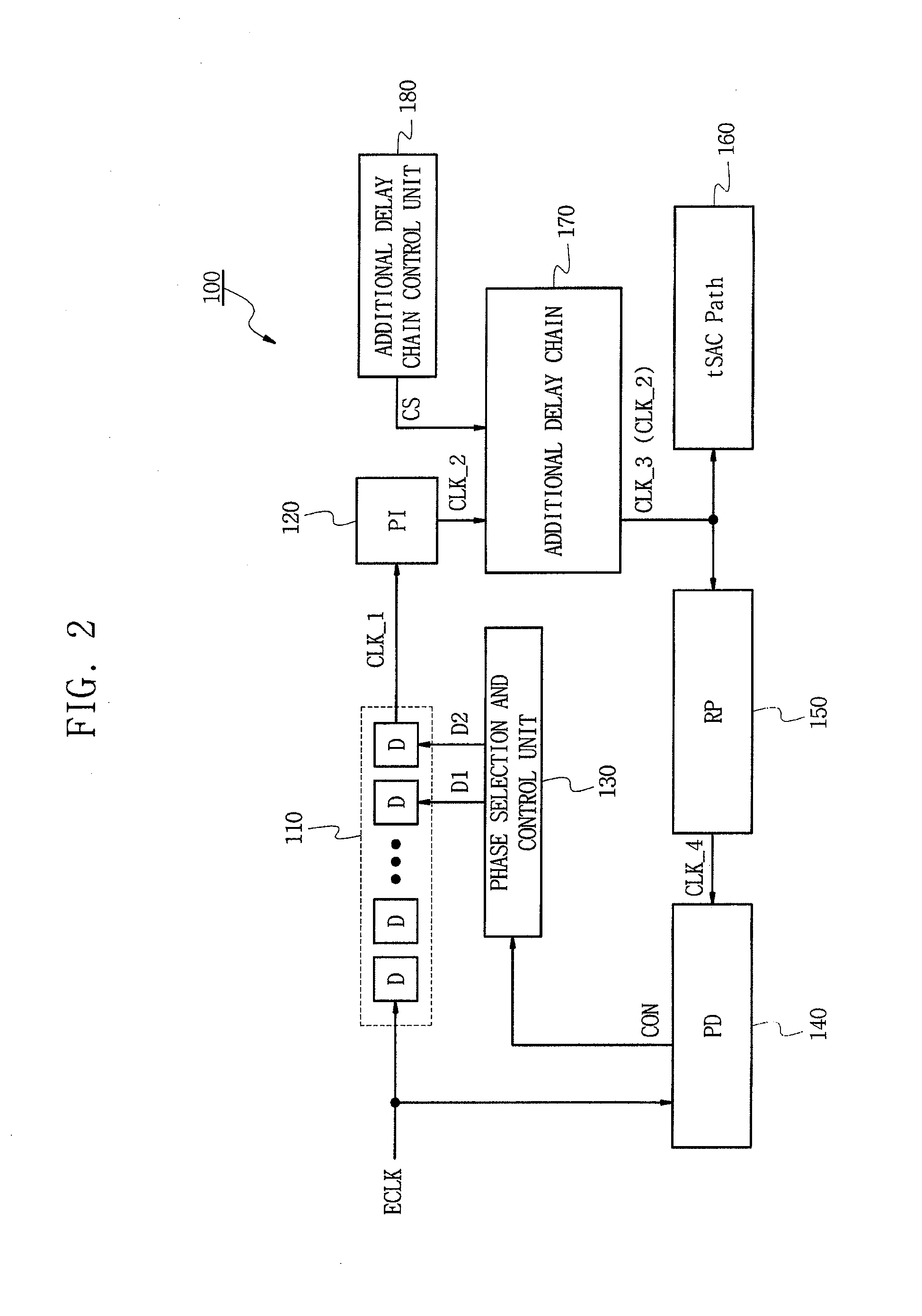
[0041]FIG. 2 is a block diagram illustrating a delay locked loop circuit 100 according to an exemplary embodiment of the present invention.

[0042]Referring to FIG. 2, the delay locked loop circuit 100 according to an exemplary embodiment of the present invention comprises a main delay chain 110, a phase interpolator (PI) 120, a phase selection and control unit 130, a phase detector (PD) 140, a replica path (RP) 150, and an additional delay chain 170. The delay locked loop circuit 10...


PUM


Abstract

A delay locked loop circuit and a method for controlling the same including a delay locked loop (DLL) circuit for receiving an external clock signal and generating an internal clock signal synchronized to the external clock signal includes at least two delay chains having different types of delay cells for delaying the external clock signal. Thus, the layout area and power consumption can be reduced, and logic failures can be prevented or minimized by replacement or compensation of the main delay cells.

Description

CROSS-REFERENCE TO RELATED APPLICATION[0001]This application claims the benefit of Korean Patent Application No. 10-2007-0003122, filed Jan. 11, 2007, the disclosure of which is hereby incorporated herein by reference in its entirety.BACKGROUND OF THE INVENTION[0002]1. Technical Field[0003]The present disclosure relates to a delay locked loop circuit and a method for controlling the same and, more particularly, to a delay locked loop circuit and a method for controlling the same that are capable of compensating for delay according to voltage variations.[0004]2. Discussion of Related Art[0005]With the rapid development of semiconductor technology, digital systems such as personal computers, personal digital assistants (PDAs), and portable communication devices have been advanced in capabilities over the past several years. The operational speed and data transmission rate of peripheral devices, such as memories, communication devices, or graphic devices have also been improved. Becaus...

Claims


Application Information

Patent Timeline
IPC IPC(8): H03L7/06
CPCH03L7/10H03L7/0814H03L7/0816A47L1/15
Inventor KIM, JUN-BAEBAE, CHANG-HYUNG
Owner SAMSUNG ELECTRONICS CO LTD
Why Eureka
Try Eureka