Low-voltage-drop rectifier circuit

a rectifier circuit and low-voltage drop technology, applied in logic circuit coupling/interface arrangement, pulse technique, instruments, etc., can solve the problem of not having a schottky diode availabl

Active Publication Date: 2019-02-19
VIA ALLIANCE SEMICON CO LTD
View PDF2 Cites 0 Cited by
  • Summary
  • Abstract
  • Description
  • Claims
  • Application Information

AI Technical Summary

Benefits of technology

[0004]In a preferred embodiment, the invention is directed to a low-voltage-drop rectifier circuit with an input node and an output node, including: a first MOSFET (Metal Oxide Semiconductor Field Effect Transistor), wherein the first MOSFET has a gate terminal for receiving a control voltage, a source terminal connected to a connection node, a drain terminal coupled to the input node, and a body terminal connected to the connection node, and wherein the input node is arranged for receiving an input voltage; a second MOSFET, wherein the second MOSFET has a gate terminal for receiving the control voltage, a source terminal coupled to the output node, a drain terminal connected to the connection node, and a body terminal connected to the output node, and wherein the output node is arranged for outputting an output voltage; a comparator, comparing the input voltage with the output voltage, so as to generate a first comparison voltage and a second comparison voltage; and a level adjustment circuit, generating and fine-tuning the control voltage according to the first comparison voltage and the second comparison voltage, wherein when the first MOSFET and the second MOSFET are both turned on, the output voltage is equal to the input voltage minus a voltage drop substantially between 0.1V and 0.2V.

Problems solved by technology

However, the Schottky diode is not available using a general CMOS (Complementary Metal Oxide Semiconductor) manufacturing process.

Method used


Image

  • Low-voltage-drop rectifier circuit
  • Low-voltage-drop rectifier circuit
  • Low-voltage-drop rectifier circuit

Examples


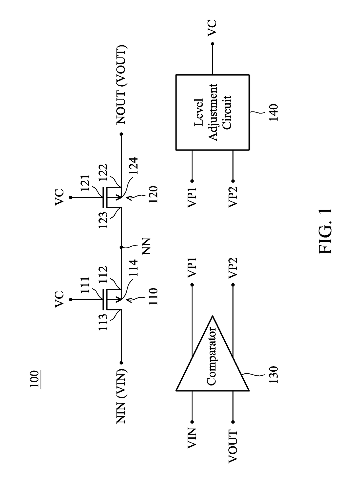
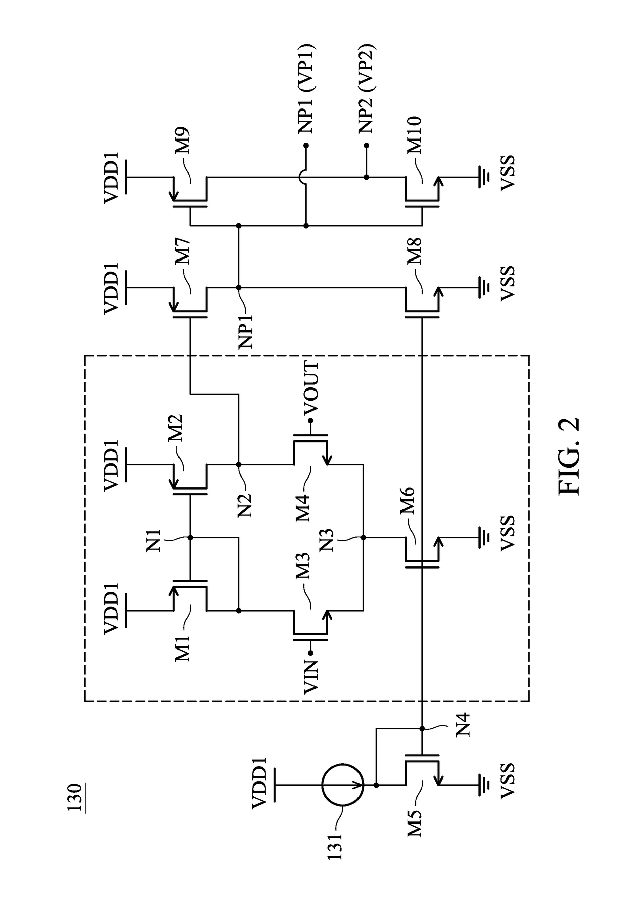
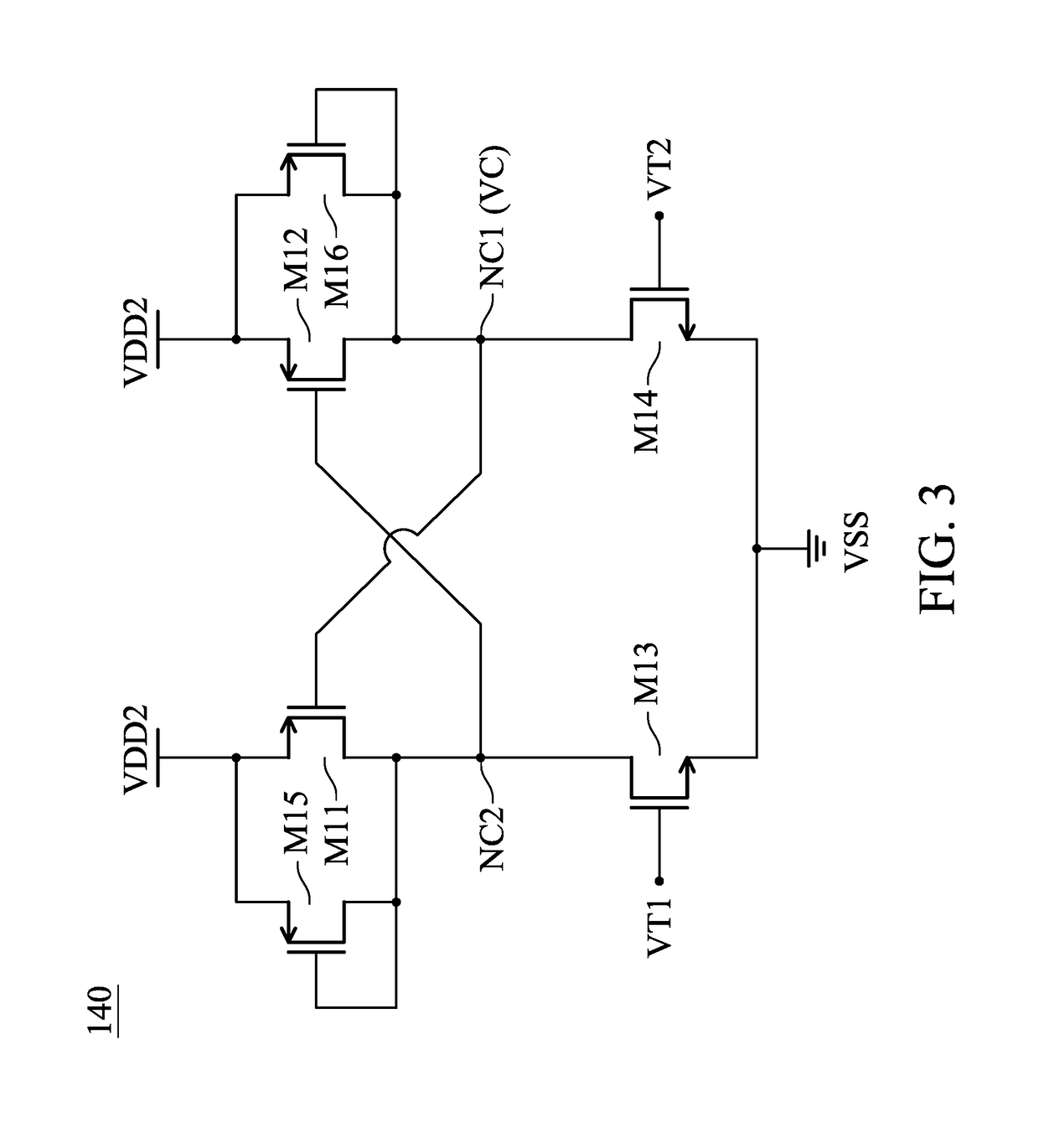
Embodiment Construction

[0022]In order to illustrate the purposes, features and advantages of the invention, the embodiments and figures of the invention are described in detail as follows.

[0023]Certain terms are used throughout the description and following claims to refer to particular components. As one skilled in the art will appreciate, manufacturers may refer to a component by different names. This document does not intend to distinguish between components that differ in name but not function. In the following description and in the claims, the terms “include” and “comprise” are used in an open-ended fashion, and thus should be interpreted to mean “include, but not limited to . . . ”. The term “substantially” means the value is within an acceptable error range. One skilled in the art can solve the technical problem within a predetermined error range and achieve the proposed technical performance. Also, the term “couple” is intended to mean either an indirect or direct electrical connection. According...


PUM


Abstract

A low-voltage-drop rectifier circuit includes a first MOSFET (Metal Oxide Semiconductor Field Effect Transistor), a second MOSFET, a comparator, and a level adjustment circuit. The first MOSFET has a gate terminal for receiving a control voltage, a source terminal connected to a connection node, a drain terminal connected to an input node, and a body terminal connected to the connection node. The second MOSFET has a gate terminal for receiving the control voltage, a source terminal connected to an output node, a drain terminal connected to the connection node, and a body terminal connected to the output node. The comparator generates a first comparison voltage and a second comparison voltage according to an input voltage at the input node and an output voltage at the output node. The level adjustment circuit generates and fine-tunes the control voltage according to the first comparison voltage and the second comparison voltage.

Description

BACKGROUND OF THE INVENTIONField of the Invention[0001]The disclosure generally relates to a low-voltage-drop rectifier circuit, and more specifically, to a low-voltage-drop rectifier circuit used as a Schottky diode.Description of the Related Art[0002]The Schottky diode, named after German physicist Walter Schottky, is popularly used in power circuits. A traditional diode has a semiconductor-to-semiconductor junction, and its forward bias voltage is about 0.6V to 0.7V. In comparison, a Schottky diode has a metal-to-semiconductor junction, and its forward bias voltage is merely about 0.1V to 0.2V. The characteristics of the Schottky diode are more similar to those of an ideal diode than a traditional diode.[0003]However, the Schottky diode is not available using a general CMOS (Complementary Metal Oxide Semiconductor) manufacturing process. If a Schottky diode is implemented with a discrete component, it will occupy a large layout area on a PCB (Printed Circuit Board). Accordingly, ...

Claims


Application Information

Patent Timeline
Patent Type & Authority Patents(United States)
IPC IPC(8): H03K19/018H03K19/0185H03K5/24H03K17/687H03K19/20H02M3/158
CPCH03K19/018521H03K5/2481H03K17/6872H02M3/158H03K19/20H02M1/36H02M7/217H03F3/45076
Inventor LEE, YEONG-SHENG
Owner VIA ALLIANCE SEMICON CO LTD
Why Eureka
Try Eureka