Dual port static memory cell and semiconductor memory device having the same

Active Publication Date: 2005-03-01
SAMSUNG ELECTRONICS CO LTD
View PDF8 Cites 6 Cited by
  • Summary
  • Abstract
  • Description
  • Claims
  • Application Information

AI Technical Summary

Benefits of technology

In an effort to overcome the problems described above, it is a feature of the present invention to provide a dual port static memory cell capable of operating high speed while minimizing layout area.
It is another feature of the present invention to provide a semiconductor memory device including a dual port static memory cell capable of operating at high speed while minimizing layout area.

Problems solved by technology

However, since the conventional dual port static memory cell does not employ a pair of bit lines in the cell but only have a single bit line, a differential amplifier may not be used in the read operation.
Accordingly, there results a problem that read operation time is long in duration a data read operation.
Further, the conventional dual port static memory cell is disadvantageous in that data can be precisely written into a latch being comprised of the inverters 11 and I2 as long as a boosted voltage which is higher than a power supply voltage VCC is applied to the word line WL during a write operation.
Accordingly, a differential amplifier cannot be used for a read operation and therefore data read time is long.
As a result, there results a problem that noise margin decreases.
However, there is a problem that as a size of a transistor increases, layout area of the transistor also increases.

Method used


Image

  • Dual port static memory cell and semiconductor memory device having the same
  • Dual port static memory cell and semiconductor memory device having the same
  • Dual port static memory cell and semiconductor memory device having the same

Examples


Embodiment Construction

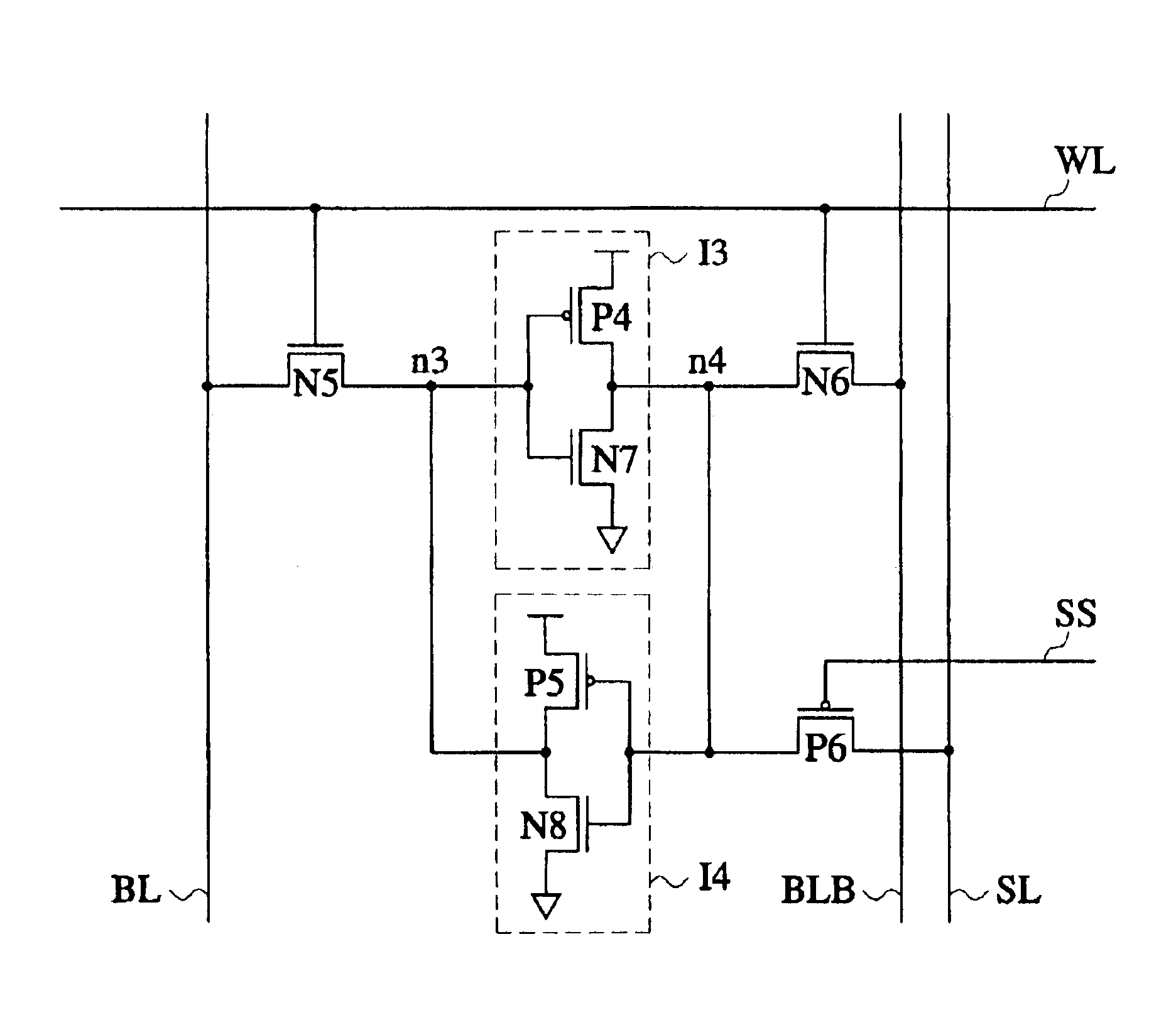
FIG. 4 illustrates a circuit diagram of a dual port static memory cell in accordance with the present invention. Referring to FIG. 4, a dual port static memory cell of the present invention comprises NMOS transistors N5, N6, N7 and N8, and PMOS transistors P4, P5 and P6.

Operation of the circuit in FIG. 4 will be described below.

It is assumed for purposes of description of the invention using an illustrative example that a logic “low” level data and a logic “high” level data are input to a node n3 and node n4, respectively, during a write operation.

Then, during a pre-charge operation, a pair of bit lines BL / BLB are charged to logic “high” level, and a scan bit line SL is pre-discharged to logic “low” level.

In this situation, if a read operation and a scan (read) operation are performed simultaneously, logic “high” level is asserted to a word line WL and logic “low” level is asserted to a scan control line SS, so that the NMOS transistors N5 and N6 and the PMOS transistors P6 are turn...


PUM


Abstract

The present invention includes a dual port static memory cell and a semiconductor memory device having the same, the dual port static memory cell comprising a first transmission gate having a gate connected to a word line and connected between a bit line and a first node, a second transmission gate having a gate connected to the word line and connected between a complementary bit line and a second node, a latch connected between the first node and the second node, and a PMOS transistor having a gate connected to a scan control line and connected between the second node and a scan bit line.

Description

BACKGROUND OF INVENTION1. Field of the InventionThe present invention relates to a static random access memory (SRAM), and particularly to a dual port static memory cell and a semiconductor memory device including the same.2. Description of Related ArtGenerally, a conventional dual port static memory cell comprises a word line, a pair of bit lines and six transistors connected between a scan control line and a scan bit line so that a read operation and a scan (read) operation may be simultaneously performed.FIG. 1 illustrates a conventional dual port static memory cell comprising NMOS transistors N1, N2, N3 and N4, and PMOS transistors P1 and P2.Referring to FIG. 1, the NMOS transistor N1 has a gate connected to a word line WL, a source (drain) connected to a node n1 and a drain (source) connected to a bit line BL. The PMOS transistor P1 and the NMOS transistor N3 form an inverter I1, and the inverter I1 is connected between the node n1 and a node n2. The PMOS transistor P2 and the ...

Claims


Application Information

Patent Timeline
IPC IPC(8): G11C8/16G11C8/00G11C11/41
CPCG11C8/16G11C11/41G11C11/417
Inventor KIM, TAE-HYOUNGSONG, TAE-JOONG
Owner SAMSUNG ELECTRONICS CO LTD
Why Eureka
Try Eureka