NAND flash memory device having facing bar and method of fabricating the same

a technology of flash memory and facing bar, which is applied in the direction of semiconductor devices, basic electric elements, electrical appliances, etc., can solve the problems of affecting the overall affecting the operation of the device, and increasing the trap charge loss ratio, so as to improve the overall operation characteristics, reduce the layout area, and facilitate the extension of the transmission channel length of the transistor.

Active Publication Date: 2019-05-16
DOSILICON CO LTD
View PDF5 Cites 0 Cited by
  • Summary
  • Abstract
  • Description
  • Claims
  • Application Information

AI Technical Summary

Benefits of technology

[0006]The present invention is directed to a NAND flash memory device with improved overall operating characteristics by minimizing a layout area and easily extending lengths of transmission channels of transistors forming a cell string, and a method of fabricating the same.

Problems solved by technology

Thus, phenomena, such as a short channel effect, a leakage current of a silicon substrate, gate induced drain leakage (GIDL), drain induced barrier lowering (DIBL), program disturbances, and a rise in trap charge loss ratio, occur in the conventional NAND flash memory device.
Problems, such as a variation in threshold voltage due to interference between adjacent cell transistors, occur.

Method used


Image

  • NAND flash memory device having facing bar and method of fabricating the same
  • NAND flash memory device having facing bar and method of fabricating the same
  • NAND flash memory device having facing bar and method of fabricating the same

Examples


Embodiment Construction

[0016]Exemplary embodiments of the present invention will be described in detail below with reference to the accompanying drawings. While the present invention is shown and described in connection with the exemplary embodiments thereof, it will be apparent to those skilled in the art that various modifications can be made without departing from the spirit and scope of the invention.

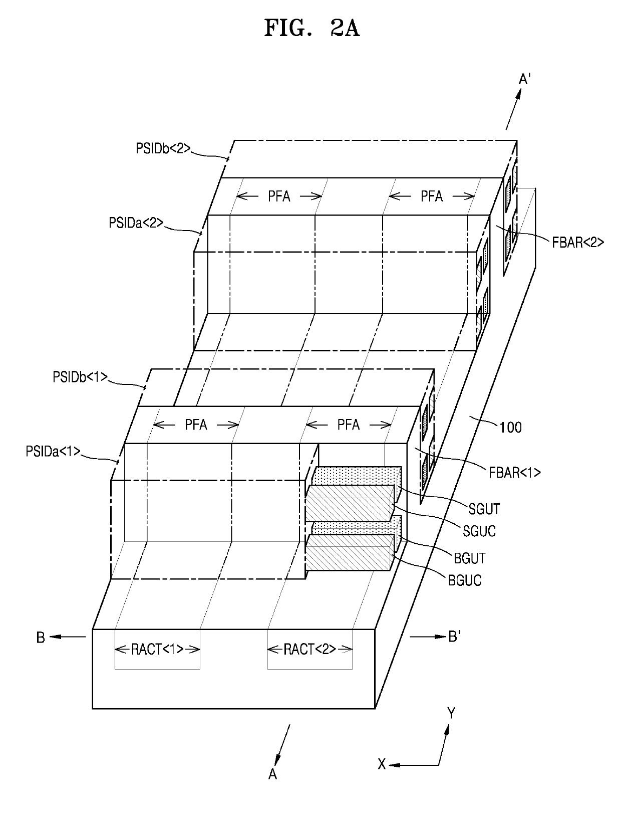
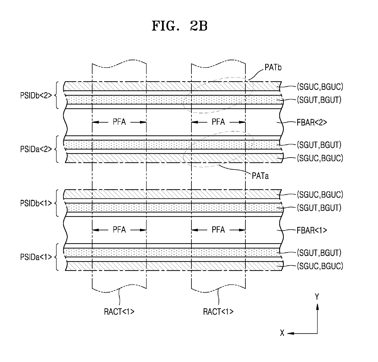
[0017]FIGS. 2A and 2B are conceptual views of a NAND flash memory device according to an exemplary embodiment of the present invention, which are respectively a perspective view and a plan view of a portion of a cell string array. In FIGS. 2A and 2B, for the sake of clarity, only main components are illustrated.

[0018]Referring to FIGS. 2A and 2B, the NAND flash memory device of the present invention includes a facing bar FBAR and first and second side structures PSIDa and PSIDb.

[0019]At least one facing bar FBAR is included in the NAND flash memory device according to the present invention. For example, a...


PUM


Abstract

A NAND flash memory device having a facing bar and a method of fabricating the same are provided. The method includes forming one transistor or a plurality of stack transistors as cell transistors on two side surfaces of a facing bar to have transmission channels thereat. In this case, the height of the facing bar may be easily increased. Thus, not only a layout area of unit transistors including the cell transistors but also a layout area of cell strings may be minimized, and lengths of the transmission channels of the cell transistors may be sufficiently extended. As a result, according to the NAND flash memory device and the method of fabricating the same, the overall operating characteristics are improved.

Description

CROSS-REFERENCE TO RELATED APPLICATION[0001]This application claims priority to and the benefit of Korean Patent Application No. 2017-0152296, filed on Nov. 15, 2017, the disclosure of which is incorporated herein by reference in its entirety.BACKGROUND1. Field of the Invention[0002]The present invention relates to a NAND flash memory device and a method of fabricating the same, and more particularly, to a NAND flash memory device having a facing bar and a method of fabricating the device.2. Discussion of Related Art[0003]As shown in FIG. 1, a NAND flash memory device, which is one type of non-volatile memory device, includes a string array STARR in which a plurality of cell strings STG<1:m> are arranged. Each of the cell strings STG<1:m> includes a drain select transistor DST, a plurality of cell transistors MC<1:n>, and a source select transistor SST, which are connected in series between a corresponding one of bit lines BL<1:m> and a common source line CSL...

Claims


Application Information

Patent Timeline
Patent Type & Authority Applications(United States)
IPC IPC(8): H01L27/1157H01L27/11565H01L29/792H01L29/66H01L21/762
CPCH01L27/1157H01L27/11565H01L29/792H01L29/66833H01L21/762H01L29/7926H10B43/10H10B43/27H10B41/35H10B41/42H10B41/50H10B43/35H10B43/50
Inventor KIM, JIN HOKANG, TAE GYOUNG
Owner DOSILICON CO LTD
Why Eureka
Try Eureka