Structure of test area for a semiconductor tester

a technology of semiconductor tester and test area, applied in the field of semiconductor tester, can solve the problems of reducing throughput, time delay, damage to the test circuit,

Inactive Publication Date: 2008-07-24
KING YUAN ELECTRONICS
View PDF5 Cites 6 Cited by
  • Summary
  • Abstract
  • Description
  • Claims
  • Application Information

AI Technical Summary

Problems solved by technology

However, if the DUT is not fine, it would cause damages to the test circuit.
However, the back and forth movement may cause time delay and reduce the throughput.
The increase on the frequencies of transferring the DUT is in company with the increase of attachment between the DUT and the socket and damages on the DUT to raise the cost.

Method used


Image

  • Structure of test area for a semiconductor tester
  • Structure of test area for a semiconductor tester
  • Structure of test area for a semiconductor tester

Examples


Embodiment Construction

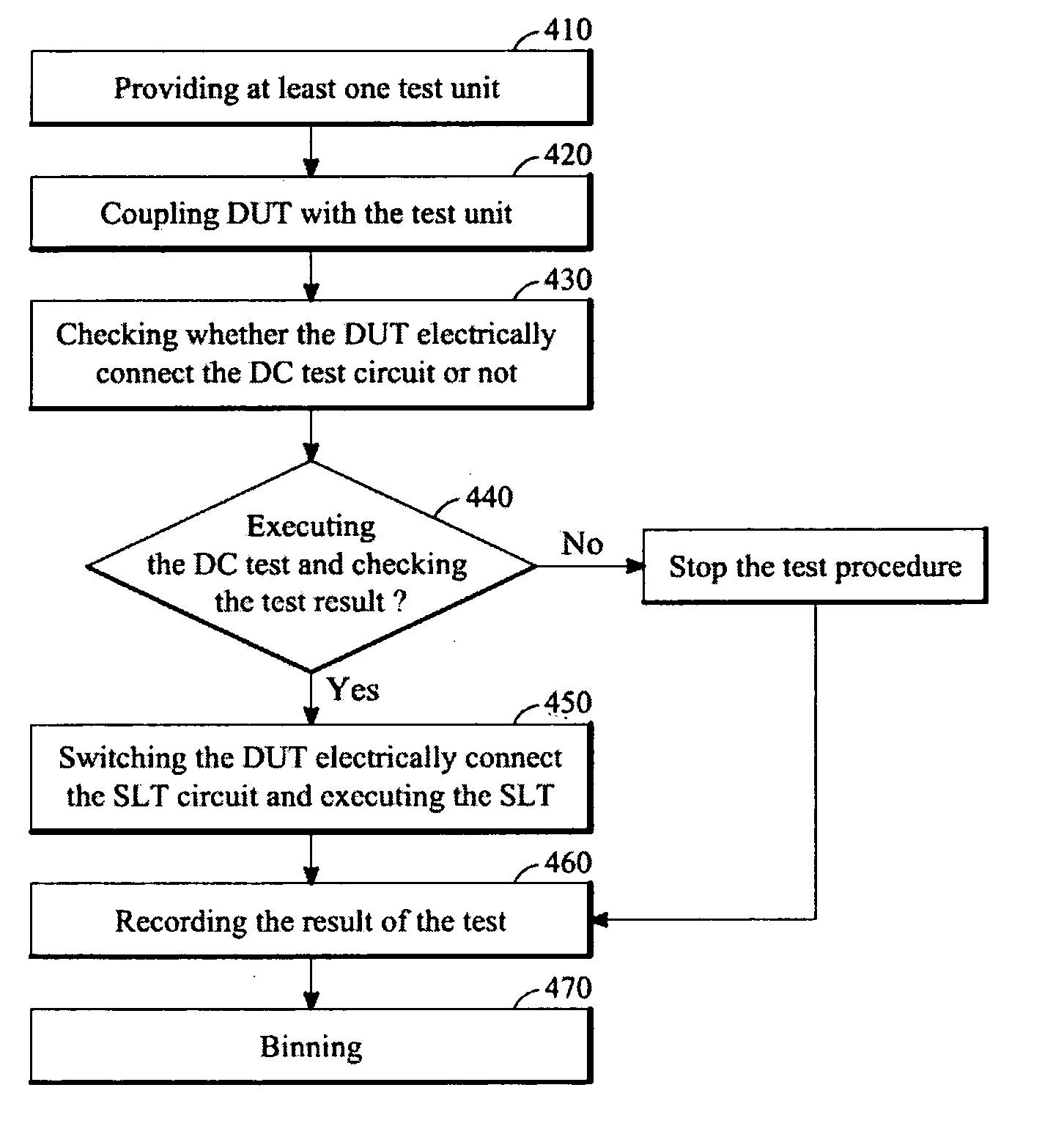
[0017]Devices and methods for DC test and SLT (system level test) integration are disclosed in the present invention; especially, the aperture of the test area is emphasized. For clear and bright, it would be described of the steps and the combinations particularly. It is not limited to perform the present invention only on the special details of the DC test and the SLT. Besides, what is well known to those skilled in the art of the semiconductor tester and methods is not described in detail for preventing the unnecessary limitations. The preferred embodiments of the present invention will be described as follow, but except the preferred embodiments, the present inventions could perform in other embodiments. And the scope of the present invention is not limited by the description; it all by what we claim later.

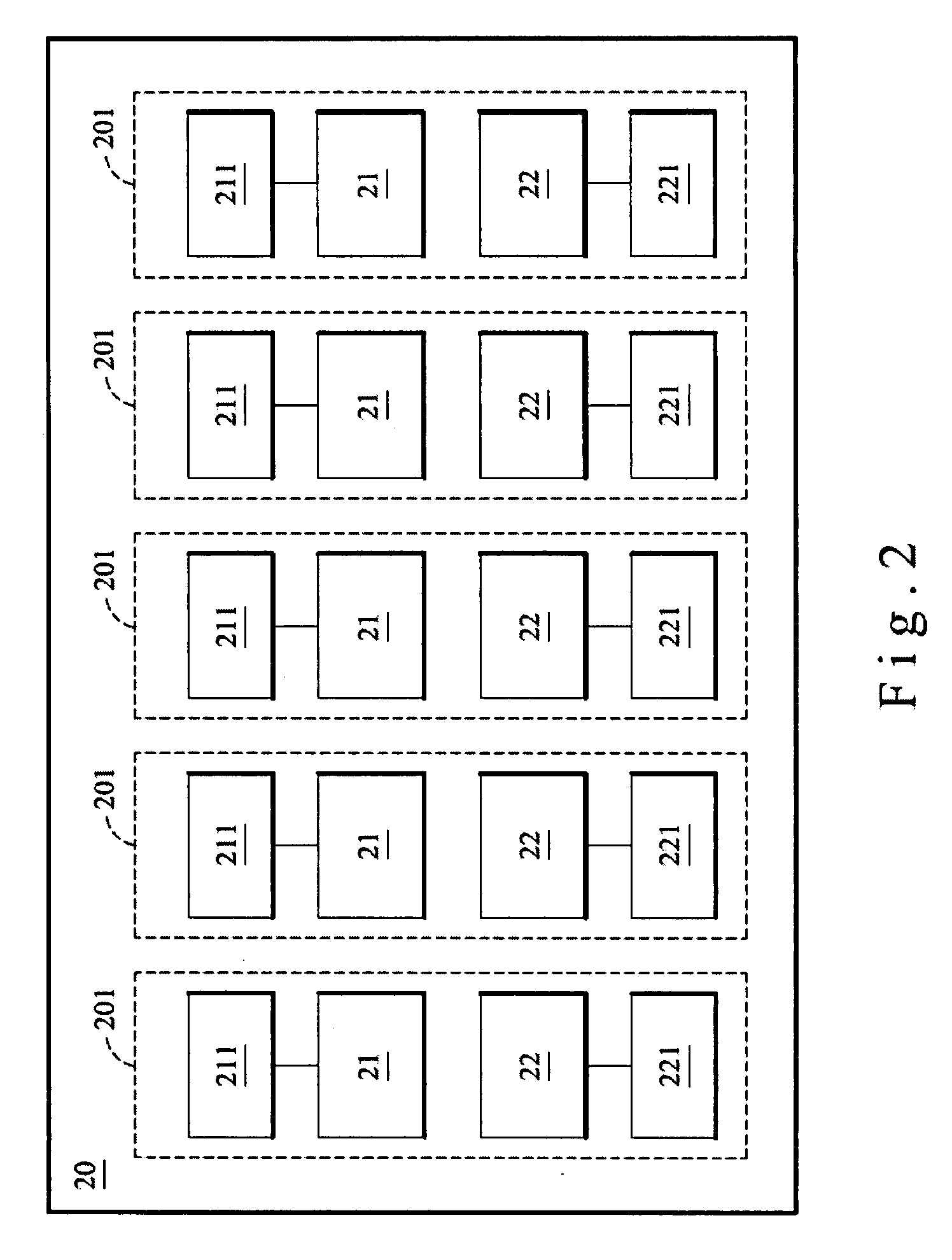
[0018]FIG. 2 is a schematic diagram illustrating the structure of the test area according to one embodiment of the present invention. As FIG. 2 shown, the test area 20 include...


PUM


Abstract

Devices and methods for DC and SLT (system level test) integration are disclosed. The DC circuit and the SLT circuit are integrated into the same device. Therefore, the DUT (device under testing) can precede the SLT before the FT (final test) when the DUT passes the DC.

Description

BACKGROUND OF THE INVENTION[0001]1. Field of the Invention[0002]The present invention relates to semiconductor tester, and more particularly, to devices and methods for DC test and SLT (system level test) integration.[0003]2. Description of the Related Art[0004]The semiconductor test is to check and make sure the function of IC, named Device Under Test / DUT as well, to be complete, and the IC can be binned by the result of test.[0005]However, if the DUT is not fine, it would cause damages to the test circuit. Therefore, DUT is supposed to be performed the DC test first, for example, the open / short circuit test. After ascertaining the DUT as regular, the DUT would be held with the help of the robot of a handler and moved to the SLT circuit test area for the SLT.[0006]FIG. 1 is a schematic diagram illustrating the conventional configuration of a semiconductor tester in a test area. A DUT is held by the robot of a handler and moved from the tray of the input port to the DC test socket 1...

Claims


Application Information

Patent Timeline
Patent Type & Authority Applications(United States)
IPC IPC(8): G01R31/26
CPCG01R1/04G01R31/2886G01R31/2834G01R1/206
Inventor YUAN-CHI, LINHSIEH, CHIH-HUNGLIN, SHIH-FANGPAN, HAO-HSIN
Owner KING YUAN ELECTRONICS
Why Eureka
Try Eureka