Test equipment, method for loading test plan and program product

a test equipment and test program technology, applied in the direction of automated test systems, testing circuits, instruments, etc., can solve the problems of increasing the size of the test plan program, the inability of conventional semiconductor testers to simulate a test program, and the cost of semiconductor manufacturing for developmen

Inactive Publication Date: 2010-10-05
ADVANTEST CORP
View PDF9 Cites 36 Cited by
  • Summary
  • Abstract
  • Description
  • Claims
  • Application Information

AI Technical Summary

Problems solved by technology

The most part of cost in manufacturing semiconductor is for development and maintenance of a test program for testing an integrated circuit for practicability and functionality.
That is, a conventional semiconductor tester has little or no capability to simulate a test program.
That causes a big problem that testing of the device needs to catch up with such trends of advancement and complication in functionality and also needs to improve capability of analyzing a device to shorten a turn around time (TAT).
Accordingly, as more and more functions are incorporated into such devices, the size of the test plan program is increasing.
That not only adds to a load of development of the test plan program but also increase a time required to load the test plan program to test equipment.
When various models of devices are manufactured by a small number for each model or if different models of devices need to be tested in a day, time will be consumed just for loading the test plan program.

Method used


Image

  • Test equipment, method for loading test plan and program product
  • Test equipment, method for loading test plan and program product
  • Test equipment, method for loading test plan and program product

Examples


Embodiment Construction

[0031]Embodiments of the present invention will be described in detail below. Like numerals are given to like elements and the redundant description will be omitted. The embodiments shown below merely provide examples for describing the present invention and do not intend to limit the present invention thereto. Various modifications and applications are possible for the present invention without departing from the spirit of the invention.

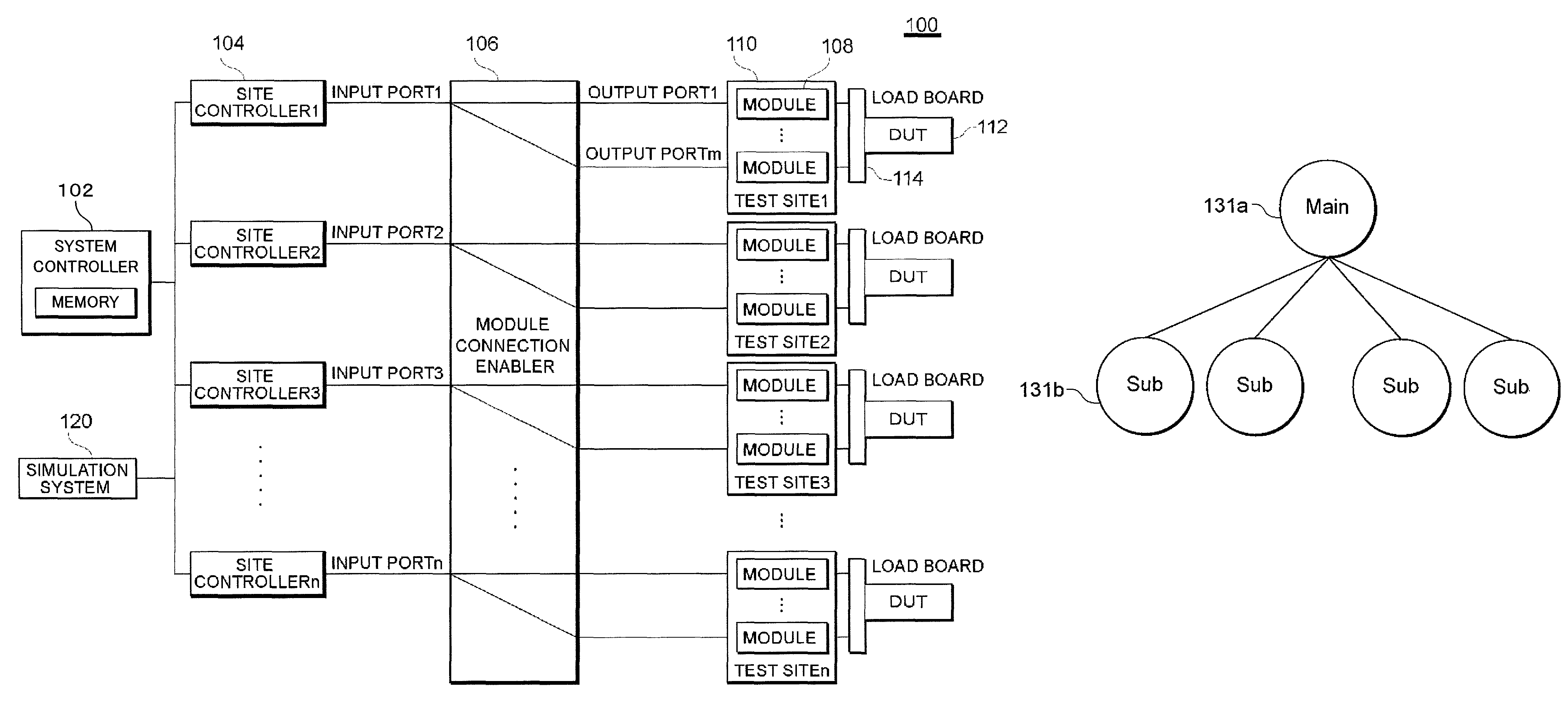
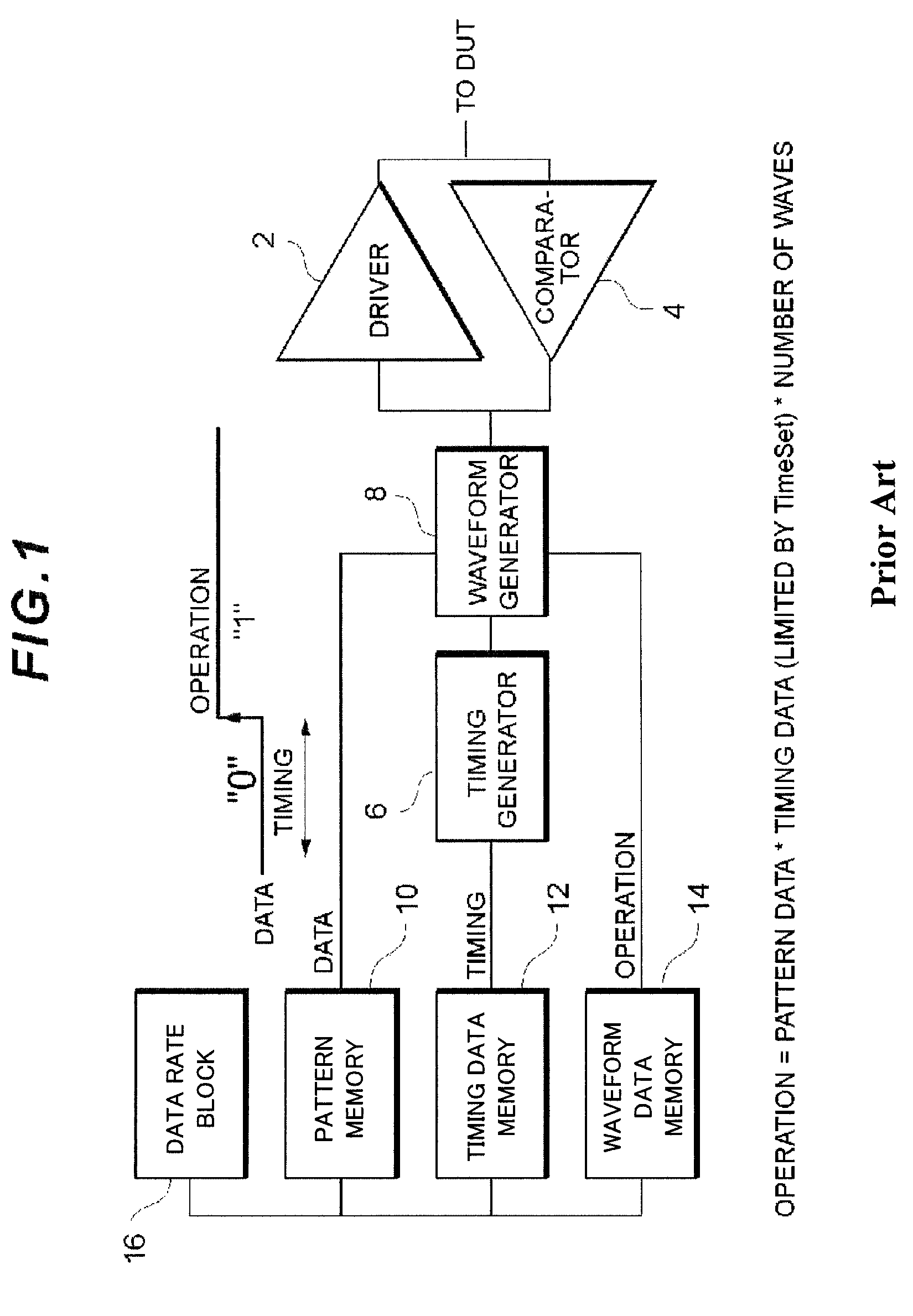
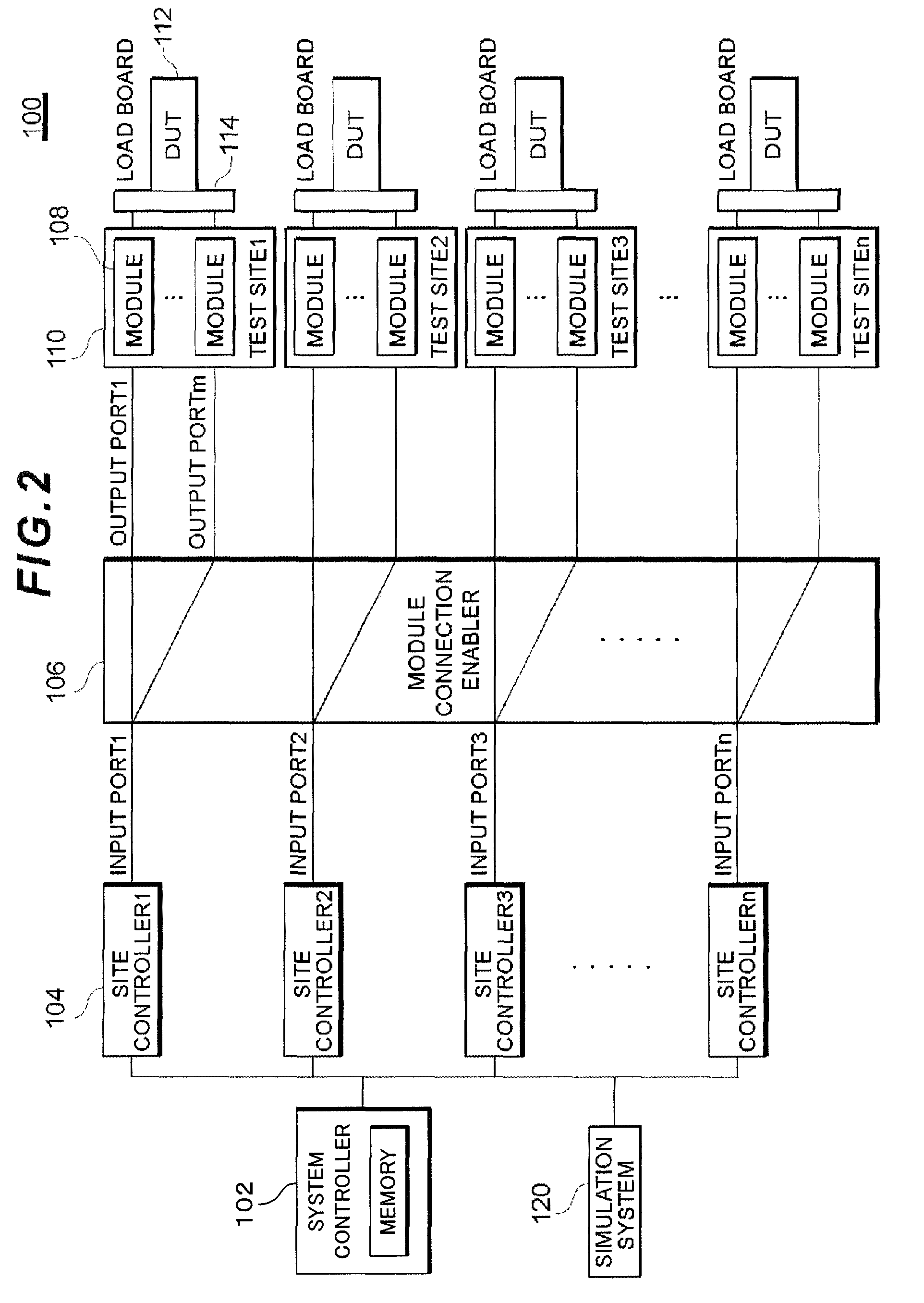
[0032]FIG. 1 illustrates a generalized architecture of a conventional tester showing how a signal is generated and applied to a device-under-test (DUT). Each DUT input pin is connected to a driver 2 that applies test data, while each DUT output pin is connected to a comparator 4. In most cases, tri-state driver-comparators are used so that each tester pin (channel) can act either as an input pin or as an output pin. The tester pins dedicated to a single DUT collectively form a test site that works with an associated timing generator 6, waveform gene...


PUM


Abstract

Test equipment includes a memory to which a test plan that includes a plurality of sub-test plans is loaded and a system controller that, when the test equipment actually examines a device-under-test (DUT), loads the test plan to the memory by the unit of the sub-test plan and supplies a test signal to the DUT by interpreting the loaded test plan.

Description

BACKGROUND OF THE INVENTION[0001]1. Field of the Invention[0002]The present invention relates to the field of automated test equipment (ATE). In particular, the present invention relates to a technique of loading of a test plan in the ATE for semiconductor testing.[0003]2. Description of the Related Art[0004]The most part of cost in manufacturing semiconductor is for development and maintenance of a test program for testing an integrated circuit for practicability and functionality. Many hours of operations on actual tester hardware have been needed for the purpose of performing the development and maintenance. That is, a conventional semiconductor tester has little or no capability to simulate a test program. Under such restriction, an engineer is forced to debug his / her test program in the actual tester hardware.[0005]Recently, an emulator for test equipment has been provided. Accordingly, functionality of a test program can be verified without requiring the use of any high-priced...

Claims


Application Information

Patent Timeline
Patent Type & Authority Patents(United States)
IPC IPC(8): G01R31/00G01R31/14
CPCG01R31/31718G01R31/318314G01R31/31907G01R31/2834
Inventor ADACHI, TOSHIAKI
Owner ADVANTEST CORP
Why Eureka
Try Eureka