Electroconductive laminate, electromagnetic wave shielding film for plasma display and protective plate for plasma display

a technology electroconductive film, which is applied in the direction of optical elements, instruments, coatings, etc., can solve the problems of limited lamination number of oxide layer and metal layer lamination, increased internal stress of electromagnetic wave shielding film, and increased thickness of metal layer in electroconductive film. , to achieve the effect of excellent electrical conductivity, excellent electrical conductivity and small resistivity of electroconductive film

Inactive Publication Date: 2008-07-24
ASAHI GLASS CO LTD
View PDF12 Cites 49 Cited by
  • Summary
  • Abstract
  • Description
  • Claims
  • Application Information

AI Technical Summary

Benefits of technology

[0012]The electroconductive laminate of the present invention has a broad transmission/reflection band since the total thickness of all metal layer(s) is small and the resistivity of the electroconductive film is small, and further has excellent electrical conductivity (electromagnetic wave shielding properties), visible light transparency and near infrared shielding properties.
[0013]The electromagnetic wave shielding film for a plasma display of the present invention has a broad transmission/reflection ba...

Problems solved by technology

However, if the number of lamination is increased, such problems arose that the internal stress of the electromagnetic wave shielding film increases, whereby the film curls, or the electroconductive film may be ...

Method used


Image

  • Electroconductive laminate, electromagnetic wave shielding film for plasma display and protective plate for plasma display
  • Electroconductive laminate, electromagnetic wave shielding film for plasma display and protective plate for plasma display
  • Electroconductive laminate, electromagnetic wave shielding film for plasma display and protective plate for plasma display

Examples


first embodiment

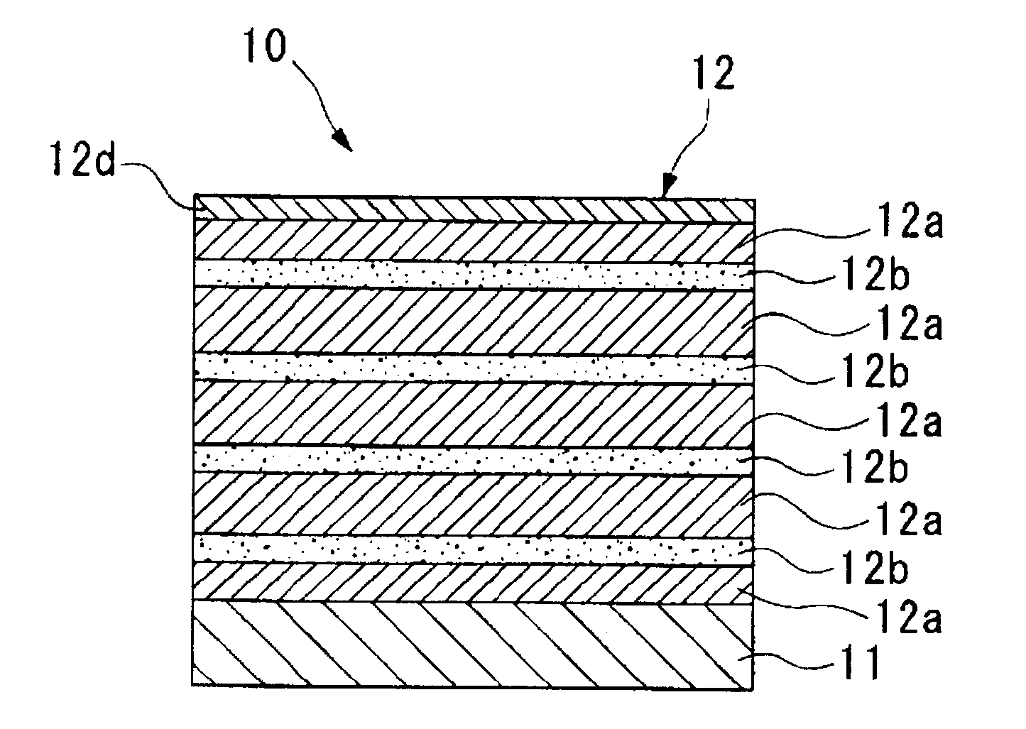
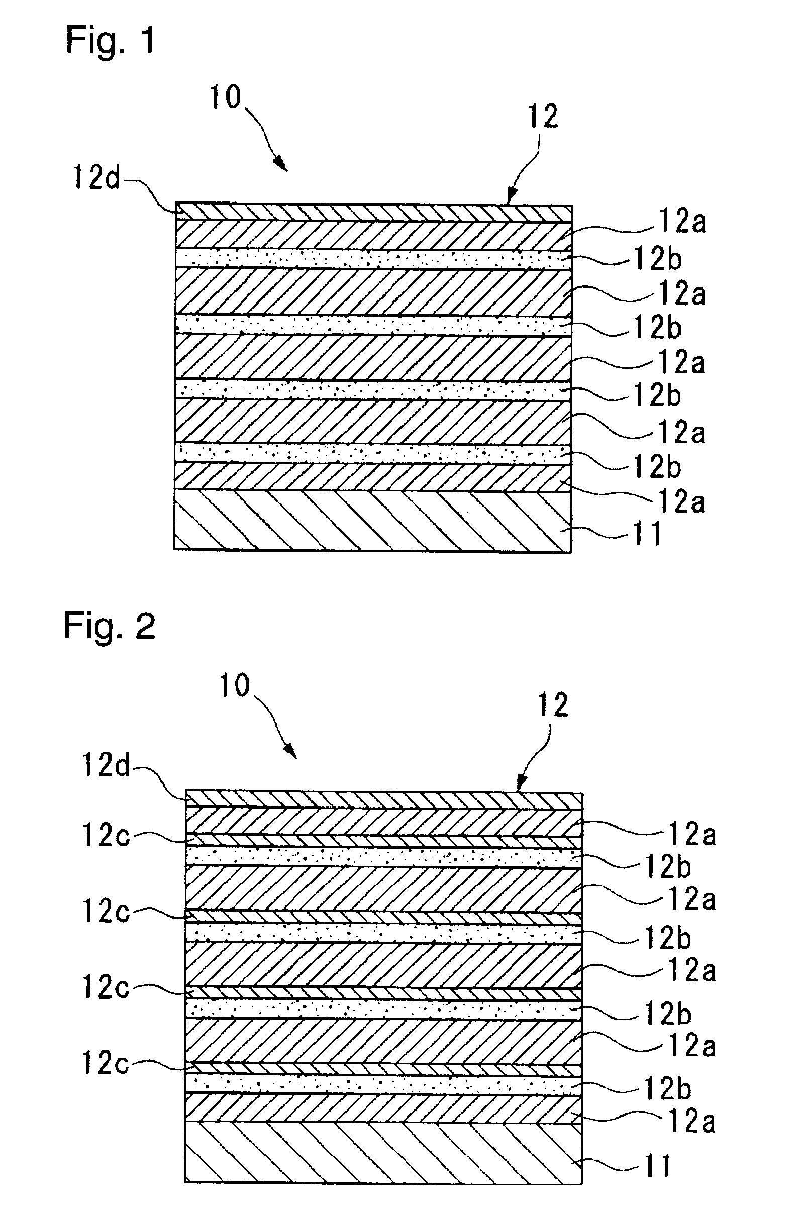
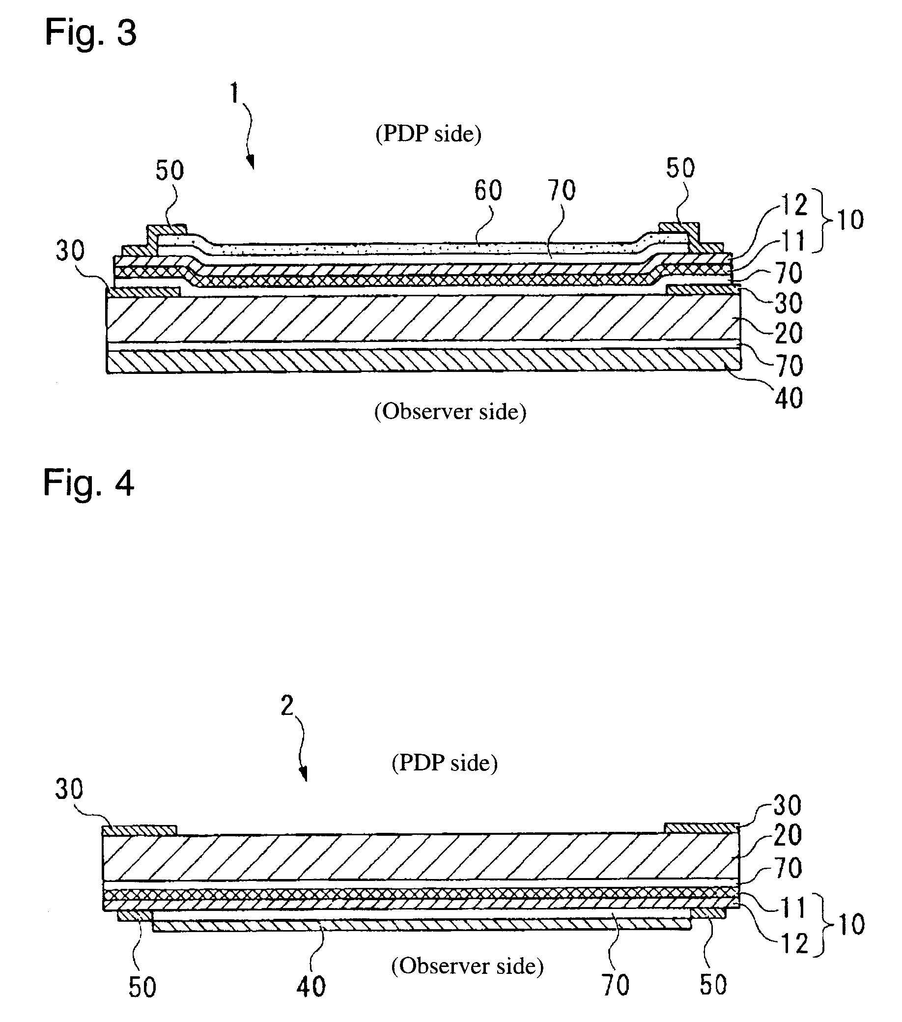
[0062]FIG. 3 illustrates a protective plate according to a first embodiment. The protective plate 1 comprises a support 20, the above electroconductive laminate 10 provided on the support 20, a color ceramic layer 30 provided at a peripheral portion on the electroconductive laminate 10 side of the support 20, a shatterproof film 40 bonded on the opposite side of the support 20 from the electroconductive laminate 10, an electrode 50 electrically in contact at a peripheral portion of the electroconductive film 12 of the electroconductive laminate 10, and a protective film 60 provided on the electroconductive laminate 10.

[0063]An adhesive layer 70 is provided between the electroconductive laminate 10 and the support 20, between the electroconductive laminate 10 and the protective film 60, and between the support 20 and the shatterproof film 40.

[0064]Further, this protective plate 1 is one having the electroconductive laminate 10 formed on the PDP side of the support 20.

(Support)

[0065]T...

second embodiment

[0077]FIG. 4 illustrates a protective plate according to a second embodiment. This protective plate 2 comprises a support 20, an electroconductive laminate 10 formed on one side of the support 20, a shatterproof film 40 formed on the electroconductive laminate 10, an electrode 50 electrically in contact with the electroconductive film 12 of the electroconductive laminate 10 at the peripheral portion, and a color ceramic layer 30 provided at a peripheral portion on the opposite side of the support 20 from the electroconductive laminate 10. Further, the shatterproof film 40 is provided inside the electrode 50.

[0078]In this embodiment, the same constituents as in the first embodiment are expressed by the same symbols as in FIG. 3 and their description is omitted.

[0079]The protective plate 2 according to the second embodiment is one having the electroconductive laminate 10 provided on the observer side of the support 20.

third embodiment

[0080]FIG. 5 illustrates a protective plate according to a third embodiment. A protective plate 3 comprises a support 20, an electroconductive laminate 10 bonded on the surface of the support 20 via an adhesive layer 70, a shatterproof film 40 bonded on the surface of the electroconductive laminate 10 via an adhesive layer 70, a color ceramic layer 30 provided at a peripheral portion on the surface of the support 20 on the opposite side from the electroconductive laminate 10, an electroconductive mesh film 80 bonded on the surface of the support 20 via an adhesive layer 70 so that a peripheral portion of the electroconductive mesh film 80 is overlaid on the color ceramic layer 30, and an electrode 90 provided at a peripheral portion of the protective plate 3 so as to electrically connect an electroconductive film 12 of the electroconductive laminate 10 to an electroconductive mesh layer (not shown) of the electroconductive mesh film 80. The protective plate 3 is an example wherein t...


PUM

PropertyMeasurementUnit
Percent by massaaaaaaaaaa
Thicknessaaaaaaaaaa
Nanoscale particle sizeaaaaaaaaaa

Abstract

An electroconductive laminate comprising a substrate and an electroconductive film formed on the substrate, wherein the electroconductive film has a multilayer structure having a high refractive index layer containing an inorganic compound and a metal layer alternately laminated from the substrate side in a total layer number of (2n+1) (wherein n is an integer of from 1 to 12); the refractive index of the inorganic compound is from 1.5 to 2.7; the metal layer is a layer containing silver; the total thickness of all metal layer(s) is from 25 to 100 nm; and the resistivity of the electroconductive film is from 2.5 to 6.0 μΩcm.

Description

BACKGROUND OF THE INVENTION[0001]1. Field of the Invention[0002]The present invention relates to an electroconductive laminate, an electromagnetic wave shielding film for a plasma display having electromagnetic wave shielding properties for shielding electromagnetic noises generated from a plasma display panel (hereinafter referred to as a PDP) provided on the observer side of the PDP to protect the PDP main body, and a protective plate for a plasma display.[0003]2. Discussion of Background[0004]Electroconductive laminates having transparency are used as a transparent electrode of e.g. a liquid crystal display device, a windshield for an automobile, a heat mirror, electromagnetic wave shielding window glass, etc. For example, Patent Document 1 discloses a coated electroconductive laminate comprising a transparent substrate, and a transparent oxide layer comprising zinc oxide and a silver layer alternately laminated on the substrate in a total layer number of (2n+1) (wherein n≧2). Su...

Claims


Application Information

Patent Timeline
IPC IPC(8): G02B1/10B32B7/02B32B9/00
CPCG02B1/116G02B5/208H05K9/0096H01J2211/446H01J11/44H05B33/14G02B1/16G02B1/11
Inventor MORIMOTO, TAMOTSUKAWASAKI, MASATOMIYAZAWA, HIDEAKI
Owner ASAHI GLASS CO LTD
Why Eureka
Try Eureka