System for accumulating exposure energy information of wafer and management method of mask for exposure utilizing exposure energy information of wafer accumulated with the system

a technology of exposure energy information and management method, which is applied in the field of system for accumulating management method of mask for exposure utilizing exposure energy information of wafer accumulated with the system, can solve the problems of inability to prevent management, crystal growth and haze development, and more serious mask defects, etc., and achieves the effect of increasing the yield of semiconductors

Active Publication Date: 2008-07-24
CYMER KOREA
View PDF10 Cites 2 Cited by
  • Summary
  • Abstract
  • Description
  • Claims
  • Application Information

AI Technical Summary

Benefits of technology

[0008]Another object of the invention is to provided a system for accumulating exposure energy information of a wafer and a management method of a mask for exposure utilizing exposure energy information of the wafer accumulated with the system in which the badness of the wafer generated due to the exposure of the wafer by means of a contaminated mask is prevented so that the yield of the semiconductor is increased.

Problems solved by technology

By the rising action like this, the mask contamination such as the crystal growth and the haze is progressed more rapidly and the more serious mask defect is generated.
According this, there are several disadvantages that the preventive management can not be performed and the yield of the semiconductor can not be increased according to the use of the contaminated mask.

Method used


Image

  • System for accumulating exposure energy information of wafer and management method of mask for exposure utilizing exposure energy information of wafer accumulated with the system
  • System for accumulating exposure energy information of wafer and management method of mask for exposure utilizing exposure energy information of wafer accumulated with the system
  • System for accumulating exposure energy information of wafer and management method of mask for exposure utilizing exposure energy information of wafer accumulated with the system

Examples


Embodiment Construction

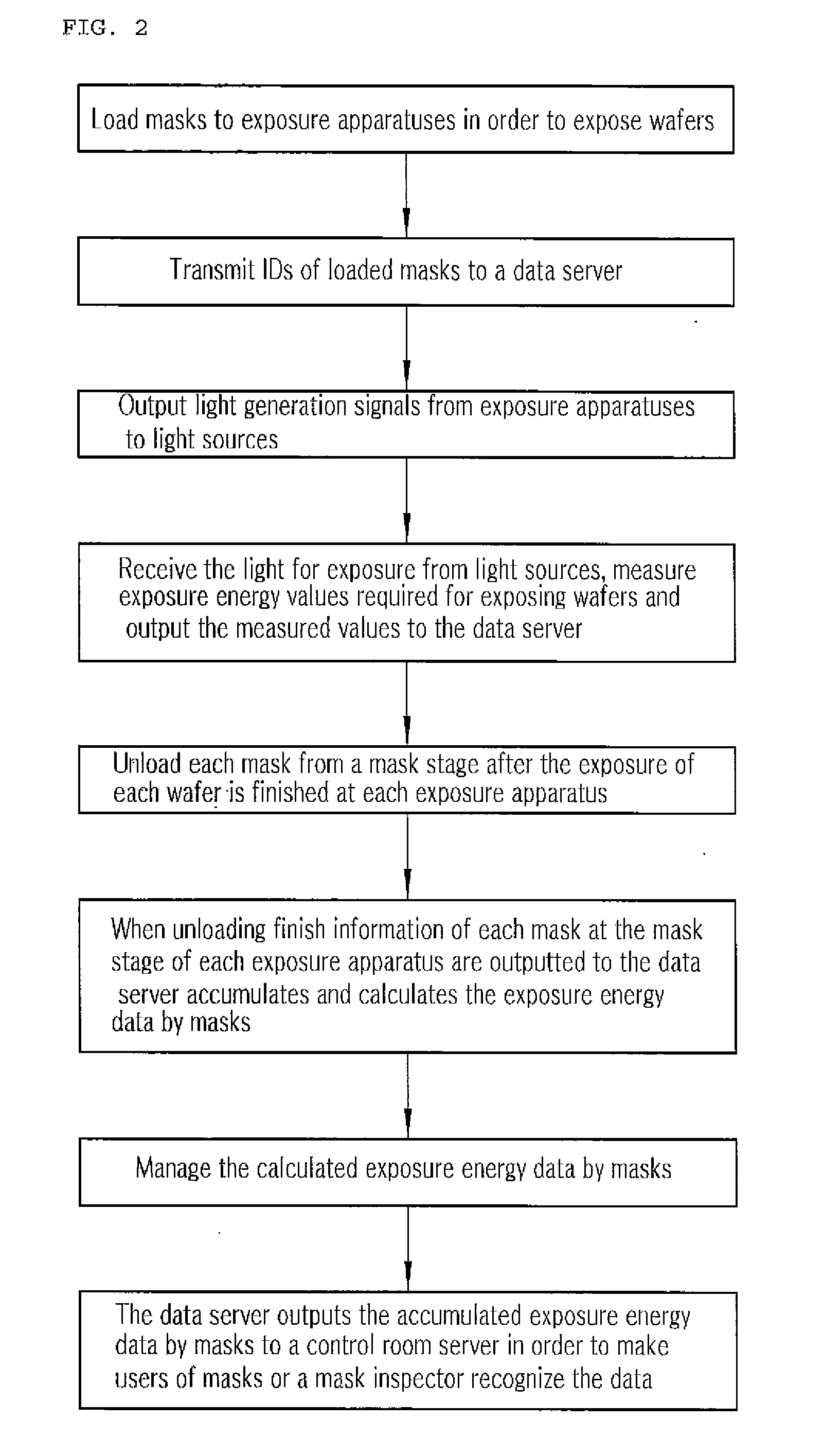
[0014]Now, the present invention will be described in detail with reference to the annexed drawings.

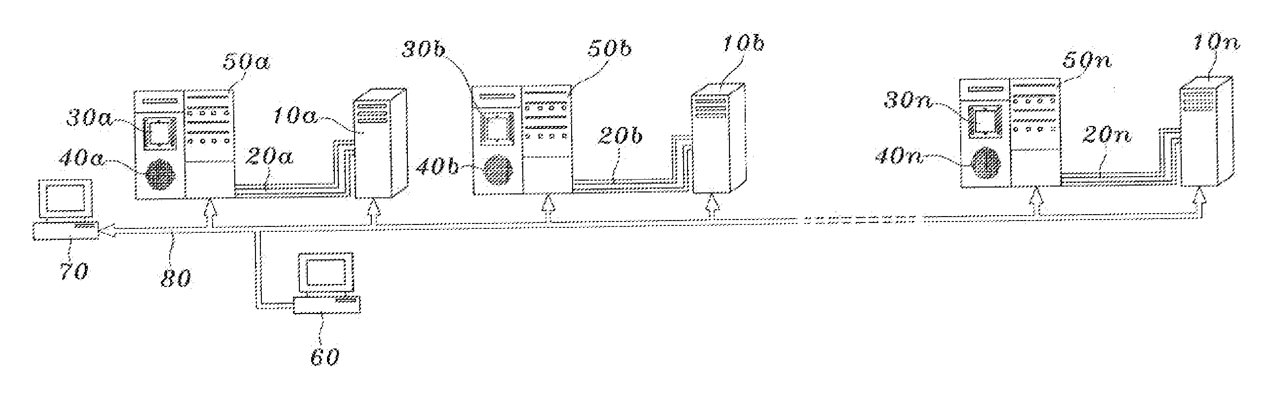
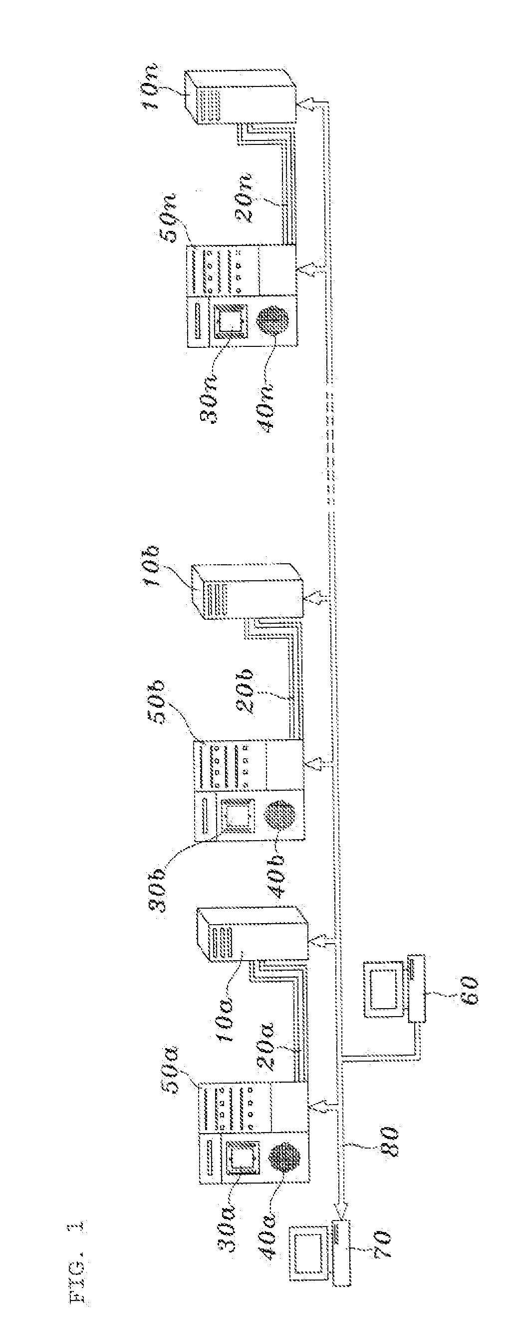
[0015]FIG. 1 is a view schematically illustrating a system for accumulating exposure energy information of a wafer according to an embodiment of the present invention.

[0016]As shown in FIG. 1, a system for accumulating exposure energy information of a wafer according to an embodiment of the present invention includes: the first to n-th light sources 10a,10b, . . . , 10n for generating light energy for exposure, the first to n-th exposure apparatuses 50a,50b, . . . , 50n for receiving the exposure light energy generated from the first to n-th light sources 10a,10b, . . . , 10n through the first to n-th light transmission systems 20a,20b, . . . , 20n including a lens and a reflection mirror and the like and then exposing wafers 40a,40b, . . . , 40n through the first to n-th exposure masks 30a,30b, . . . , 30n, a data server 60 for receiving the exposure energy values used for exposing t...


PUM

PropertyMeasurementUnit
wavelength rangeaaaaaaaaaa
diameteraaaaaaaaaa
diameteraaaaaaaaaa

Abstract

Disclosed is a management method of a mask for exposure utilizing exposure energy information of a wafer. According to the present invention, in case of exposing wafers in exposure apparatuses, information on masks loaded on exposure apparatuses are calculated from the exposure apparatuses, the light energy values applied during the exposure of wafers by the corresponding masks are calculated, the calculated light energy values are stored in the data server, the same data are collected from all wafer exposure processes performed at plural exposure apparatuses within the semiconductor FAB and the exposure information about the exposure energy relating to plural masks used by plural exposure apparatuses are accumulated and managed. Accordingly, the exposure degree of a mask about the exposure energy, as a direct cause of the contamination of masks such as the crystal growth and haze, is directly calculated and then defects of masks are predicted together with measures according that, so that deterioration of the yield of the semiconductor is prevented and the yield of the semiconductor is increased.

Description

BACKGROUND OF THE INVENTION[0001]1. Field of the Invention[0002]The present invention relates to a system for accumulating exposure energy information of a wafer and a management method of a mask for exposure utilizing exposure energy information of the wafer accumulated with the system in which in a photo lithography process of a semiconductor, the exposure degree of the mask relating to the exposure energy as direct causes of the mask contamination such as the crystal growth and haze is directly accumulated and calculated by using the light energy information caused by the wafer exposure executed by means of an original plate (mask / reticle) with a circuit patterned by an exposing apparatus such as a stepper / scanner, thereby predicting a defect of the mask and accordingly then increasing the yield of a semiconductor.[0003]2. Description of the Related Art[0004]Generally, in an exposing apparatus such as a stepper / scanner, which had been widely used conventionally, a light source su...

Claims


Application Information

Patent Timeline
Patent Type & Authority Applications(United States)
IPC IPC(8): G06K9/00G03F7/20H01L21/027
CPCG03F1/82G03F7/70916G03F7/70866G03F7/70525G03F7/70491
Inventor HONG, WOON-SIG
Owner CYMER KOREA
Why Eureka
Try Eureka