Automatic iip2 calibration architecture

a technology of automatic iip2 and calibration architecture, applied in the field of wireless communications, can solve the problems of second-order intermodulation products to appear, cumbersome methods, time-consuming and labor-intensive implementation, etc., and achieve the effect of easing testing requirements and reducing circuit overhead

Active Publication Date: 2008-07-31
ICERA CANADA ULC
View PDF3 Cites 137 Cited by
  • Summary
  • Abstract
  • Description
  • Claims
  • Application Information

AI Technical Summary

Benefits of technology

[0029]It is an object of the present invention to obviate or mitigate at least one disadvantage of previous IIP2 calibration schemes. In particular,

Problems solved by technology

A problem with this circuit lies in the non-linear nature of input transistor 54, which will generate an output y/y* having undesired intermodulation products.
This mis-match can cause the second order intermodulation products to appear.
While the previously described method of FIG. 5 is effective for testing wireless chips and systems and minimizing IIP2, it is not very practical.
In particular, the method is very cumbersome and time consuming to implement.
Moreover, relatively expensive test equipment such as signal generators and chip/system test apparatus are required.
This cost increases if high testing throughput is required, otherwise testing will be time consuming.
Therefo

Method used


Image

  • Automatic iip2 calibration architecture
  • Automatic iip2 calibration architecture
  • Automatic iip2 calibration architecture

Examples


Embodiment Construction

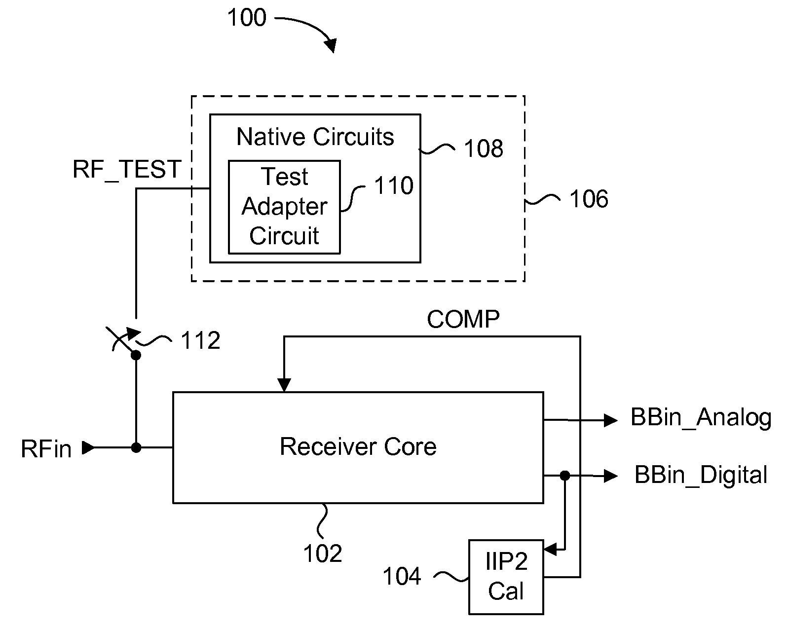
[0051]An integrated automatic IIP2 calibration architecture for wireless transceivers is disclosed. The architecture enables a wireless transceiver to generate a test radio frequency (RF) signal that will generate a second order tone with minimal additional circuitry. In particular, the test RF signal is generated using a combination of native transceiver circuits and additional test adaptor circuits. Native transceiver circuits are those circuits implemented on the transceiver chip for executing native transceiver functions during normal operation, which can be further used for generating the test (RF) signal. Test adaptor circuits are added to the transceiver chip, more specifically to the native circuits, for enabling the native circuits to generate the test RF signal in a test mode of operation. Circuits for implementing a particular IIP2 minimizing scheme can be included on the transceiver chip for automatic IIP2 calibration during the test mode of operation.

[0052]Therefore, by...


PUM


Abstract

An integrated automatic IIP2 calibration architecture for wireless transceivers is disclosed. The architecture enables a wireless transceiver to generate a test radio frequency (RF) signal having a second order tone with minimal additional circuitry. In particular, the test RF signal is generated using a combination of native transceiver circuits and test adaptor circuits. Native transceiver circuits are those circuits implemented on the transceiver chip for executing native transceiver functions during normal operation, which can be used for generating the test (RF) signal. Test adaptor circuits are added to the transceiver chip, more specifically to the native circuits, for enabling the native circuits to generate the test RF signal in a self-test mode of operation. Circuits for implementing a particular IIP2 minimizing scheme can be included on the transceiver chip for automatic IIP2 calibration during the self-test mode of operation.

Description

FIELD OF THE INVENTION[0001]The present invention relates generally to wireless communications. More particularly, the present invention relates to transceiver circuits.BACKGROUND OF THE INVENTION[0002]Wireless devices have been in use for many years for enabling mobile communication of voice and data. Such devices can include mobile phones and wireless enabled personal digital assistants (PDA's) for example. FIG. 1 is a generic block diagram of the core components of such wireless devices. The wireless core 10 includes a base band processor 12 for controlling application specific functions of the wireless device and for providing and receiving voice or data signals to a radio frequency (RF) transceiver chip 14. The RF transceiver chip 14 is responsible for frequency up-conversion of transmission signals, and frequency down-conversion of received signals. RF transceiver chip 14 includes a receiver core 16 connected to an antenna 18 for receiving transmitted signals from a base stati...

Claims


Application Information

Patent Timeline
IPC IPC(8): H04B17/00
CPCH03D2200/0045H04B17/21H04B1/12H04B1/16H04B17/00
Inventor MANKU, TAJINDERBELLAOUAR, ABDELLATIFHOLDEN, ALANSAFARI, HAMID R.
Owner ICERA CANADA ULC
Why Eureka
Try Eureka