Inductor devices

a technology of inductor and device, which is applied in the direction of inductance, printed inductance, coils, etc., can solve the problems of increasing the bandwidth of the filter, occupying an undesirably large area or exhibiting an undesirable height on the circuit board, and rendering the system more liable to nois

Inactive Publication Date: 2008-08-07
IND TECH RES INST
View PDF14 Cites 29 Cited by
  • Summary
  • Abstract
  • Description
  • Claims
  • Application Information

AI Technical Summary

Benefits of technology

[0008]Examples of the present invention may further include an inductor device comprising a first conductive pattern on a first layer of a substrate, a second conductive pattern on a second layer of the substrate, and a first region between the first layer and the second layer through which at least one hole is coupled between the first dielectric layer and the second dielectric layer, wherein a magnetic field induced by at least one of the first conductive pattern or the second conductive pattern at the first region is more intensive than that induced by at least one of the first conductive pattern or the second conductive pattern at a second region between the first conductive layer and the second conductive layer.
[0009]Examples of the present invention may additionally include an inductor device comprising a first conductive coil, a second conductive coil, and a first region through which at least one hole is provided, wherein a magnetic field induced by at least one of the first conductive coil or the second conductive coil at the first region is more intensive than that induced by at least one of the first conductive coil or the second conductive coil at a second region.

Problems solved by technology

Conventional inductors are mounted on circuit boards utilizing the surface mounting technique (SMT) or other complicated processes, and they may occupy an undesirably large area or exhibit an undesirable height on the circuit boards.
For example, an inductor with a low Q-factor may incur significant insertion loss in the pass band of a filter and may increase the bandwidth of the filter, which renders the system more liable to noise.
As another example, an inductor with a low Q-factor may incur undesirable phase noise in a resonator, which may deteriorate the quality of a communication system.
However, the above-mentioned prior art structured or processes may be complicated in certain applications.

Method used


Image

  • Inductor devices
  • Inductor devices
  • Inductor devices

Examples


Embodiment Construction

[0028]Reference will now be made in detail to the present examples of the invention illustrated in the accompanying drawings. Wherever possible, the same reference numbers will be used throughout the drawings to refer to the same or like portions.

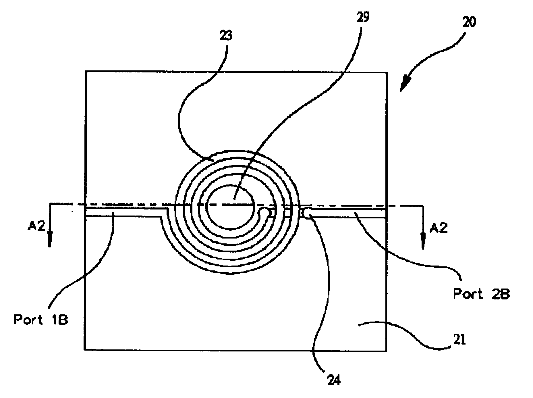
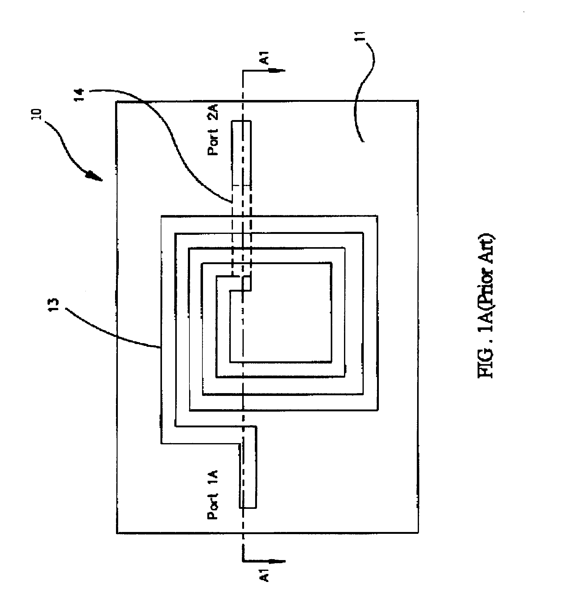
[0029]FIG. 2A, FIG. 2B and FIG. 2C are diagrams of an embedded spiral-type inductor according to an example of the present invention. FIG. 2A is a top plan view of a spiral-type inductor 20 according to an example of the present invention. Referring to FIG. 2A, the spiral-type inductor 20, formed on a multilayered substrate 21, may include a conductive coil 23 extending from a port 1B to a port 2B through a conductive path 24. In one example, the conductive coil 23 may include a plurality of connected spirals between the ports 1B and 2B. In the present example, the conductive coil 23 and the ports 1B and 2B may be formed on a top surface of the multilayered substrate 21. In other examples, such as an example illustrated in FIG. 2C, the cond...


PUM

PropertyMeasurementUnit
areaaaaaaaaaaa
dielectric loss tangentaaaaaaaaaa
relative permeabilityaaaaaaaaaa

Abstract

An inductor device comprising a first conductive pattern on a first layer of a substrate, a second conductive pattern on a second layer of the substrate, and a first region between the first layer and the second layer through which at least one hole is coupled between the first dielectric layer and the second dielectric layer, wherein a magnetic field induced by at least one of the first conductive pattern or the second conductive pattern at the first region is more intensive than that induced by at least one of the first conductive pattern or the second conductive pattern at a second region between the first conductive layer and the second conductive layer.

Description

CROSS-REFERENCE TO RELATED APPLICATIONS[0001]This application claims the benefit of U.S. Provisional Application No. 60 / 900,199, filed Feb. 7, 2007.BACKGROUND OF THE INVENTION[0002]The present invention generally relates to inductor devices and, more particularly, to embedded inductor structures with an improved quality factor.[0003]Inductors have been widely used in circuits such as resonators, filters, and impedance transformers. Conventional inductors are mounted on circuit boards utilizing the surface mounting technique (SMT) or other complicated processes, and they may occupy an undesirably large area or exhibit an undesirable height on the circuit boards. To reduce the size, embedded inductors have been developed. FIG. 1A and FIG. 1B are diagrams of an embedded spiral-type inductor in the prior art. FIG. 1A is a top plan view of a spiral-type inductor 10 in the prior art. Referring to FIG. 1A, the spiral-type inductor 10 is formed on a multilayered substrate 11 and includes a ...

Claims


Application Information

Patent Timeline
Patent Type & Authority Applications(United States)
IPC IPC(8): H01F17/00H01F5/00
CPCH01F17/0013H01F17/02H01F2017/0046H01F2017/002H01F30/08H01F2017/0073
Inventor WEI, CHANG-LINCHIN, KUO-CHIANGTSAI, CHENG-HUASHYU, CHIN-SUNCHEN, CHANG-SHENG
Owner IND TECH RES INST
Why Eureka
Try Eureka