Semiconductor device manufacturing method

Inactive Publication Date: 2008-08-07
LAPIS SEMICON CO LTD
View PDF11 Cites 11 Cited by
  • Summary
  • Abstract
  • Description
  • Claims
  • Application Information

AI Technical Summary

Benefits of technology

[0009]The present invention constructed in this way obtains advantageous effects in that a sealed structural body is not subjected to a high temperature and a structural body formed of a material low in melting point can be used.
[0010]An advantageous effect is obtained in that sealed space can be brought into high vacuum.
[0011]Further, advantageous effects are obtained in that no sealing member is deposited on the structural body and the characteristic of the structural body is prevented from varying.

Problems solved by technology

The above conventional technique is however accompanied by the problem that since a high temperature of 550° C. or higher is used where the upper portion is sealed by CVD, a structure prior to such a sealing step must be set to such one as being capable of resisting the high temperature, and hence one low in melting point, such as aluminum cannot be used.
A problem also arises in that while it is desirable to bring a sealed hollow portion into high vacuum, it is difficult to cause the hollow portion to reach high vacuum where CVD is used.
Further, a problem arises in that there is a possibility that since a film is grown even around a vibrator lying inside a hollow where the upper portion is sealed by CVD (patent document 1: FIG. 14), the characteristic of the vibrator will vary.

Method used


Image

  • Semiconductor device manufacturing method
  • Semiconductor device manufacturing method
  • Semiconductor device manufacturing method

Examples


Embodiment Construction

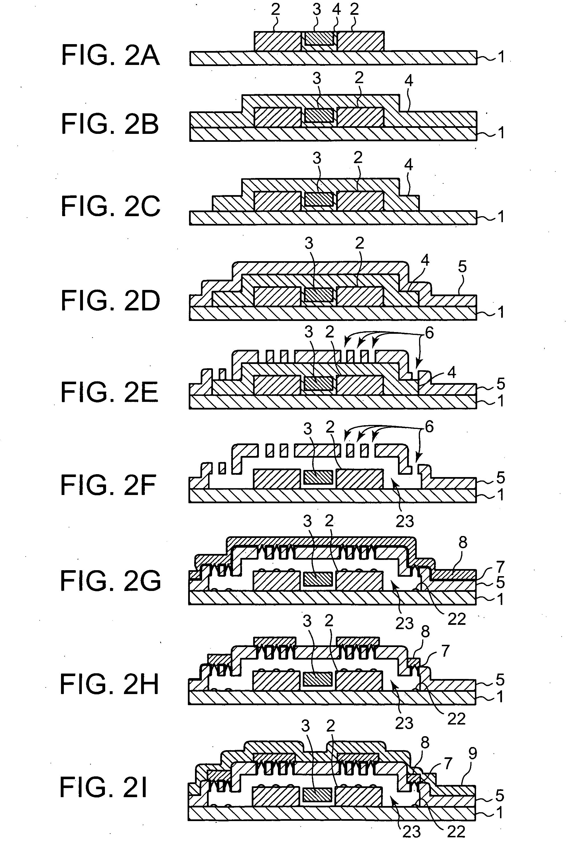
[0017]A preferred embodiment of a semiconductor device manufacturing method according to the present invention will hereinafter be described with reference to the accompanying drawings.

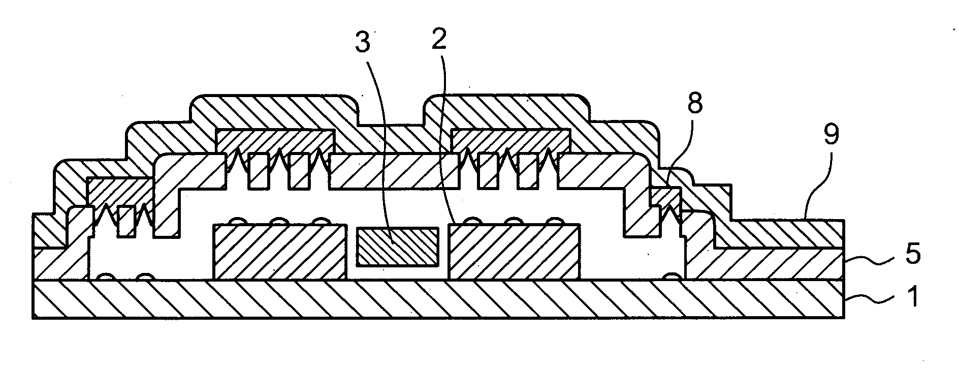
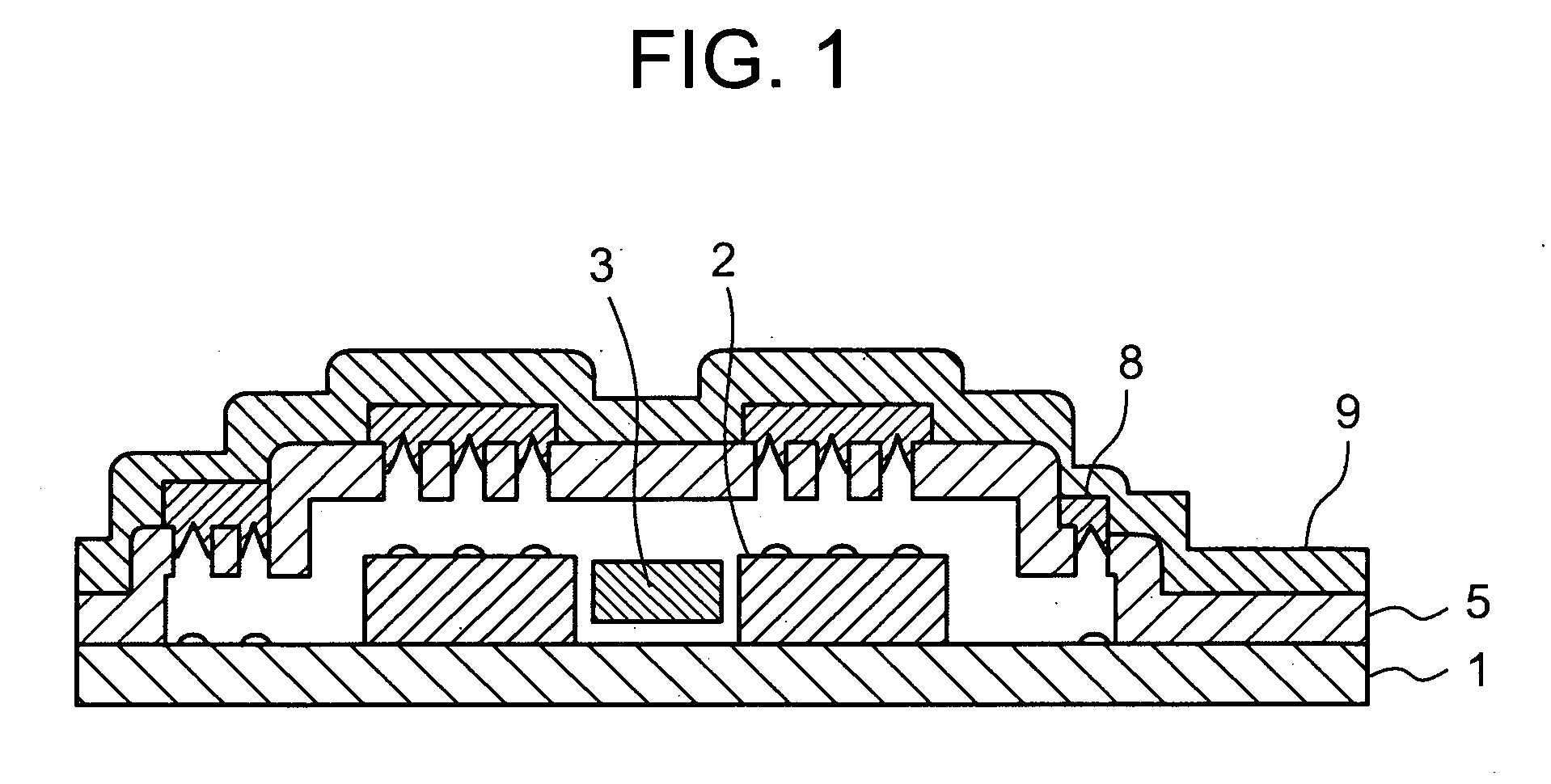
[0018]FIG. 1 is a sectional view of a semiconductor device wherein a structural body according to an embodiment is sealed.

[0019]In FIG. 1, reference numeral 1 indicates a semiconductor substrate, which has unillustrated transistors and multilayered wirings.

[0020]Reference numerals 2 indicate electrodes, which are formed on the semiconductor substrate 1 by polysilicon, silicon germanium (SiGe) or the like.

[0021]Reference numeral 3 indicates a movable structural body, which is formed on the semiconductor substrate 1 by a cantilever beam structure or a double supported beam structure or the like. The movable structural body 3 is of a vibrator and has a height that ranges from about 1 μm to 5 μm.

[0022]Incidentally, the shapes or the like of the electrodes 2 and the movable structural body 3 are not limite...


PUM


Abstract

A movable structural body formed over a semiconductor substrate is covered with a sacrifice film. The sacrifice film is covered with a silicon oxide film. Further, through holes are defined in the silicon oxide film. The sacrifice film is removed through the through holes to form space between the movable structural body and the silicon oxide film. Aluminum or an aluminum alloy high in flowability is deposited over the silicon oxide film by a sputtering method to seal the through holes.

Description

BACKGROUND OF THE INVENTION[0001]The present invention relates to a method for manufacturing a semiconductor device such as a MEMS (Micro Electric Mechanical System) device or the like wherein a mechanical element part such as a vibrator, a sensor, an actuator, an electronic circuit, and the like are integrated on one substrate.[0002]As a conventional semiconductor device manufacturing method, there is known one in which a sacrifice film deposited around a vibrator corresponding to a structural body (mechanical element part) disposed on a substrate is removed and thereafter a portion above the vibrator is sealed by depositing an oxide film by CVD (Chemical Vapor Deposition) (refer to, for example, a patent document 1 (Specification of U.S. Pat. No. 5,188,983)).[0003]The above conventional technique is however accompanied by the problem that since a high temperature of 550° C. or higher is used where the upper portion is sealed by CVD, a structure prior to such a sealing step must be...

Claims


Application Information

Patent Timeline
IPC IPC(8): H01L21/56
CPCB81B7/0041B81C2203/0136H01L21/56H01L23/315H01L2924/0002H01L2924/00
Inventor NAKAMURA, MAKIKO
Owner LAPIS SEMICON CO LTD
Why Eureka
Try Eureka