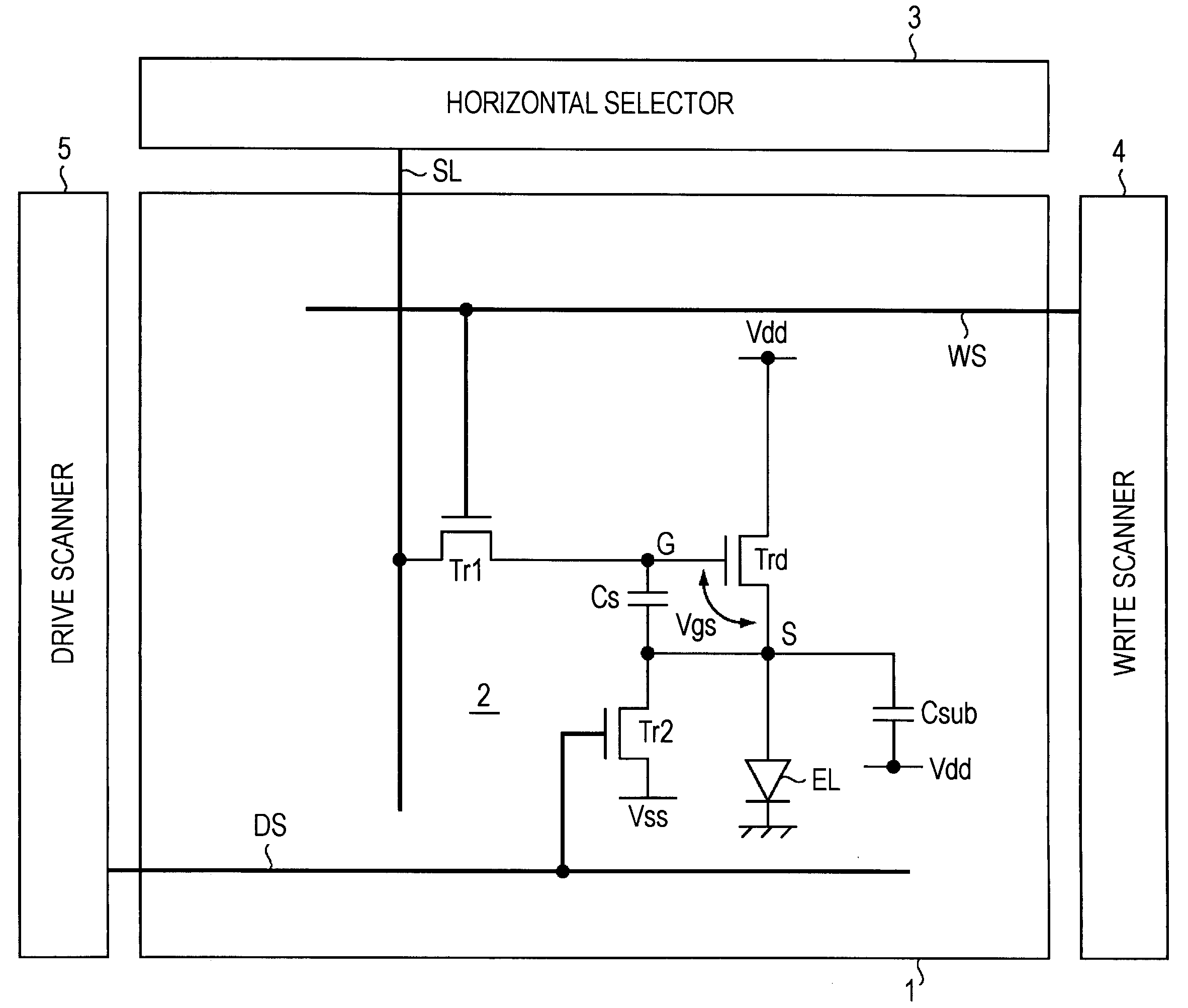
[0011]As is apparent from the transistor characteristic expression, when a thin film transistor operates in the saturation region, if the gate voltage Vgs becomes greater than the threshold voltage Vth, the transistor goes into an ON state, and the drain current Ids flows. In principle, as shown by the above-described transistor characteristic expression, if the gate voltage Vgs is constant, the same amount of the drain current Ids is supplied to the light emitting device. Accordingly, if a video signal of the same level is supplied to each pixel constituting a screen, all the pixels emit light at the same luminance, and thus the uniformity of the screen should be obtained.
[0017]According to an embodiment of the present invention, there is provided a display apparatus including: a pixel array section; and a drive section; driving the pixel array section, wherein the pixel array section includes a row of first scanning lines and second scanning lines, a column of signal lines, and pixels in a matrix, each of the pixels disposed at an intersection of each of the first scanning lines and each of the signal lines, the drive section outputs control signals to the row of first scanning lines and second scanning lines, respectively, to perform line progressive scanning on the pixels for each row, and supplies a signal potential and a predetermined off potential to a column of signal lines in synchronism with the line progressive scanning, the pixel includes a light-emitting device, a sampling transistor, a driving transistor, a switching transistor, and a holding capacitor, the sampling transistor has a control terminal connected to the first scanning line and a pair of current terminals, one of the current terminals is connected to the signal line, and the other of the current terminals is connected to a control terminal of the driving transistor, the driving transistor has a pair of current terminals, one of the current terminals is connected to a power source, and the other current terminal is connected to the light emitting device, the switching transistor has a control terminal connected to the second scanning line and a pair of current terminals, one of the current terminals is connected to a fixed potential, and the other current terminal is connected to the other current terminal of the driving transistor, and the holding capacitor has one terminal connected to the control terminal of the driving transistor and the other terminal connected to the other current terminal of the switching transistor; and wherein the sampling transistor passes a current in accordance with the control signal supplied from the first scanning line, and samples a signal potential of a video signal supplied from the signal line to hold the signal potential in the holding capacitor, the driving transistor allows a drive current to flow through the light emitting device to change the device to a luminous state in accordance with the held signal potential supplied by the current from the power source, the switching transistor becomes ON in accordance with the control signal supplied from the second scanning signal in advance of the sampling of the video signal to connect the other terminal of the holding capacitor to a fixed potential to change the light emitting device to a non-luminous state, and the sampling transistor becomes ON in accordance with the other control signal supplied from the first scanning line when the switching transistor becomes ON, and takes in the OFF voltage from the signal line to apply the voltage to the control terminal of the driving transistor, thereby preventing a penetration current from flowing from the power source toward the fixed potential.
[0019]By the present invention, when the display apparatus moves from a luminous period to a non-luminous period, the switching transistor is turned ON to connect the output current terminal (source) of the driving transistor to a fixed potential, thereby cutting off the light emitting device. Thus, the drive current is stopped from flowing through the light emitting device to change the device to a non-emission state. When the light emitting device has been in the non-luminous period, each pixel performs a predetermined correction operation. However, if this state continues without change, the drive current flows to the fixed potential through the driving transistor. Thus, in the present invention, when the switching transistor is turned ON to go into the non-luminous period, the sampling transistor is turned ON to get an OFF voltage from the signal line to apply the voltage to the control terminal (gate) of the driving transistor. Thereby, the driving transistor is turned OFF. Accordingly, it is possible to block a penetration current flowing from the power source to the fixed potential. In this manner, by cutting off the driving transistor at the time of going into the non-luminous period, it is possible to eliminate a penetration current, thereby reducing the power consumption of the panel.
