Method and apparatus for placement and routing cells on integrated circuit chips

a technology of integrated circuit chips and cells, applied in the direction of instruments, computing, electric digital data processing, etc., can solve the problem that the estimated information of routed wires cannot be considered, and achieve the effect of reducing overlap, eliminating overlap, and increasing the size of the first cell

Active Publication Date: 2008-08-21
SYNOPSYS INC
View PDF8 Cites 16 Cited by
  • Summary
  • Abstract
  • Description
  • Claims
  • Application Information

AI Technical Summary

Benefits of technology

[0012]In one embodiment of the present invention, a method to layout an integrated circuit includes: placing a first cell at a first location, at which the first cell overlaps with a portion of a second cell that is placed at a second location before the first cell is place; and moving the second cell from the second location to a third location to reduce overlapping (e.g., to eliminate overlapping) with the first cell placed at the first location. In one example, the illegal placement of the first cell with overlapping is allowed when the first cell is larger than the second cell. The second location may coincide with the first location; and, in one example, the first location is determined from optimizing a design goal, which is improved when an area of overlapping between the first and second cells is reduced. In one example, the illegal placement is generated in increasing the size of the first cell; in another example, the illegal placement is generated in inserting the first cell to buffer a signal.

Problems solved by technology

These estimates do not account for the available information of routed wires, even if only a small part of an already placed and routed design is being modified.

Method used


Image

  • Method and apparatus for placement and routing cells on integrated circuit chips
  • Method and apparatus for placement and routing cells on integrated circuit chips
  • Method and apparatus for placement and routing cells on integrated circuit chips

Examples


Embodiment Construction

[0027]The following description and drawings are illustrative of the invention and are not to be construed as limiting the invention. Numerous specific details are described to provide a thorough understanding of the present invention. However, in certain instances, well known or conventional details are not described in order to avoid obscuring the description of the present invention.

[0028]Many of the methods of the present invention may be performed with a digital processing system, such as a conventional, general purpose computer system. Special purpose computers which are designed or programmed to perform only one function may also be used.

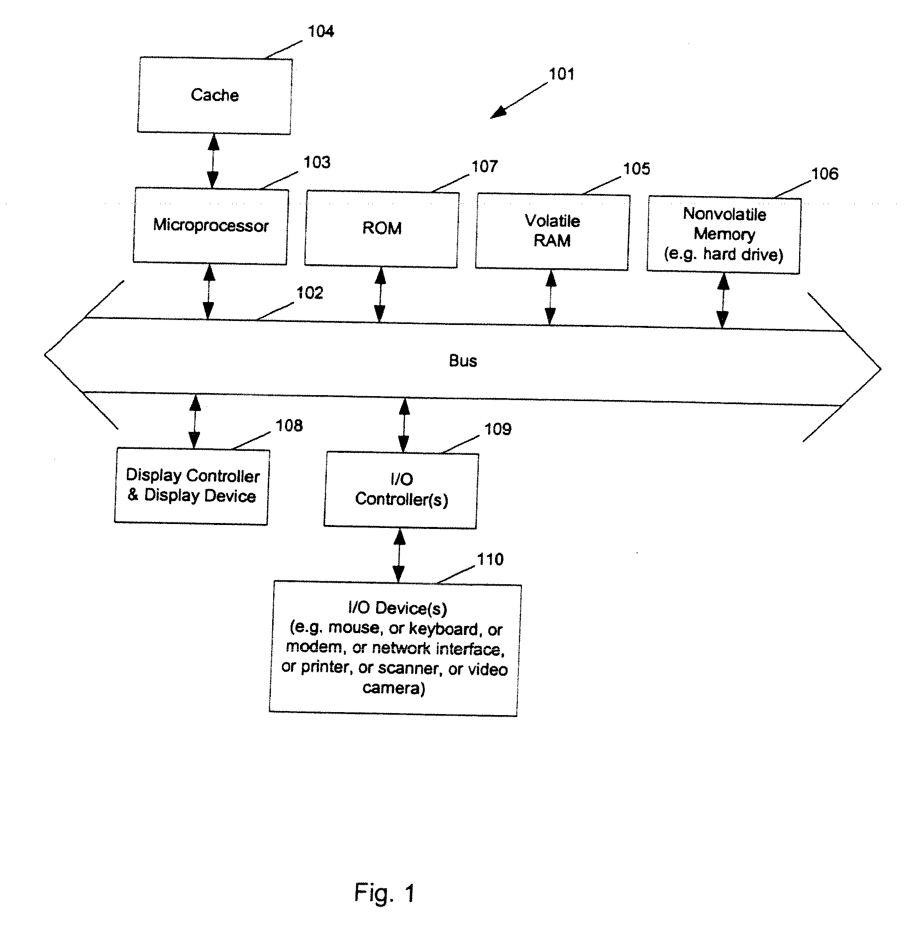
[0029]FIG. 1 shows one example of a typical computer system which may be used with the present invention. Note that while FIG. 1 illustrates various components of a computer system, it is not intended to represent any particular architecture or manner of interconnecting the components as such details are not germane to the present invention. ...


PUM


Abstract

Methods and apparatuses to place and route cells on integrated circuit chips along paths. In one aspect of the invention, methods to layout an integrated circuit are based on placing and routing cells along paths. In one embodiment, a method to layout an integrated circuit including: routing a wire to connect a first cell of the integrated circuit and a second cell of the integrated circuit; and placing a third cell of the integrated circuit after the wire is routed to connect the first cell and the second cell. In one example, the first, second and third cells are on a first path; and, the third cell is connected to one of the first and second cells on the first path by only one net. The first path is selected from a set of paths; and the first and second cells are placed before the wire is routed to connect the first cell and the second cell. Timing is analyzed using a route of the wire connecting the first cell and the second cell to select a second path from the set of paths before a cell is placed on the second path.

Description

[0001]This application is a divisional of U.S. patent application Ser. No. 10 / 351,094, filed on Jan. 23, 2003. This application also claims the benefit of the filing date of provisional application Ser. No. 60 / 388,492, filed Jun. 11, 2002, and entitled “Method and Apparatus for Placement and Routing Cells on Integrated Circuit Chips” by the inventors Roger P. Ang, Ken R. McElvain, and Kenneth S. McElvain.FIELD OF THE INVENTION[0002]The invention relates to designing integrated circuits, and more particularly to incremental placement and routing cells for integrated circuits.BACKGROUND OF THE INVENTION[0003]For the design of digital circuits on the scale of VLSI (very large scale integration) technology, designers often employ computer-aided techniques. Standard languages such as Hardware Description Languages (HDLs) have been developed to describe digital circuits to aide in the design and simulation of complex digital circuits. Several hardware description languages, such as VHDL a...

Claims


Application Information

Patent Timeline
Patent Type & Authority Applications(United States)
IPC IPC(8): G06F17/50
CPCG06F17/5031G06F17/5081G06F17/5077G06F17/5072G06F30/3312G06F30/392G06F30/394G06F30/398
Inventor ANG, ROGER P.MCELVAIN, KEN R.MCELVAIN, KENNETH S.
Owner SYNOPSYS INC
Why Eureka
Try Eureka