Substrate processing apparatus
- Summary
- Abstract
- Description
- Claims
- Application Information
AI Technical Summary
Benefits of technology
Problems solved by technology
Method used
Image

Examples
Embodiment Construction
[0034]The present invention will now be described in detail with reference to the drawings showing a preferred embodiment thereof.
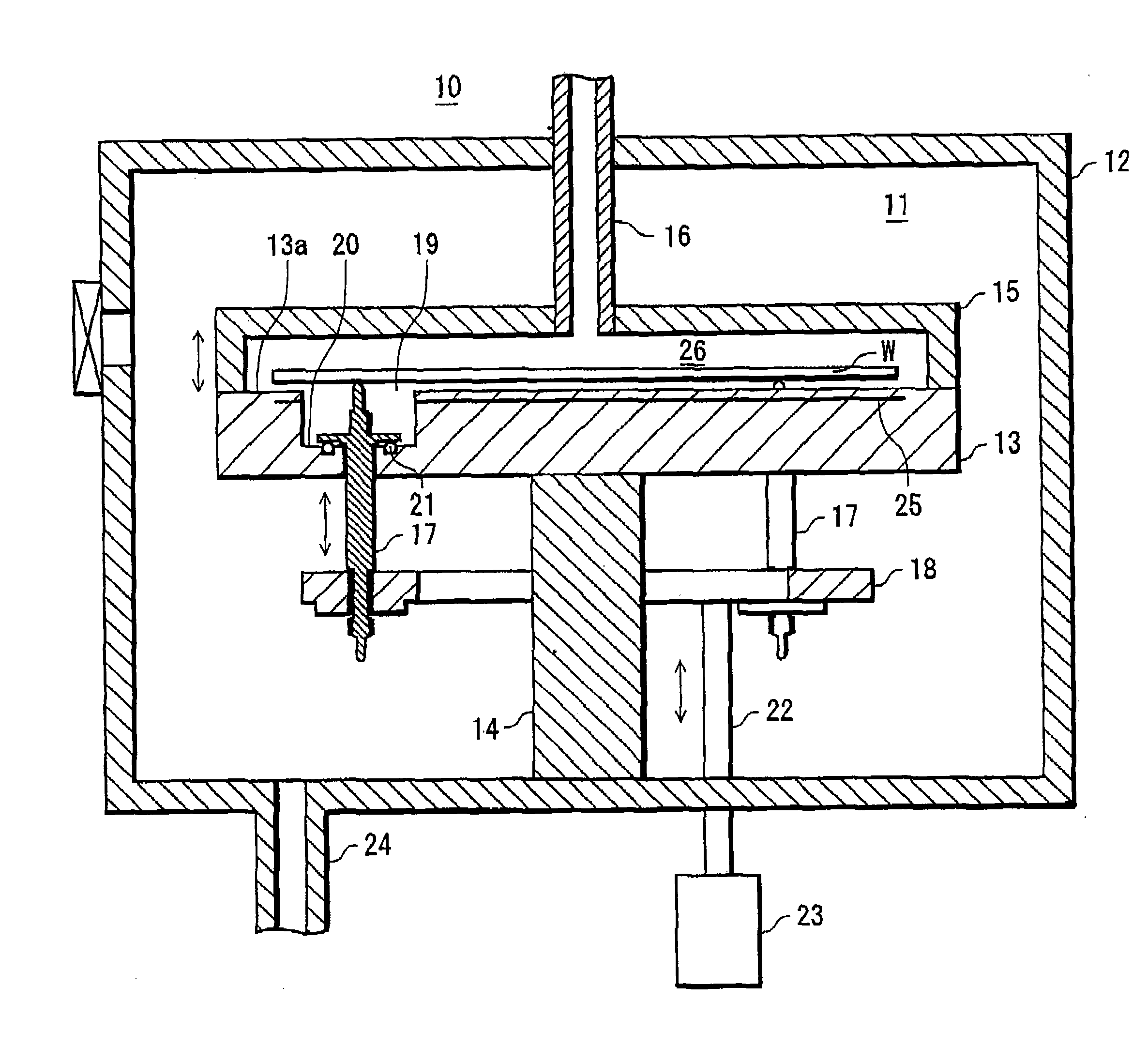
[0035]FIG. 1 is a sectional view schematically showing the construction of a substrate processing apparatus according to an embodiment of the present invention.
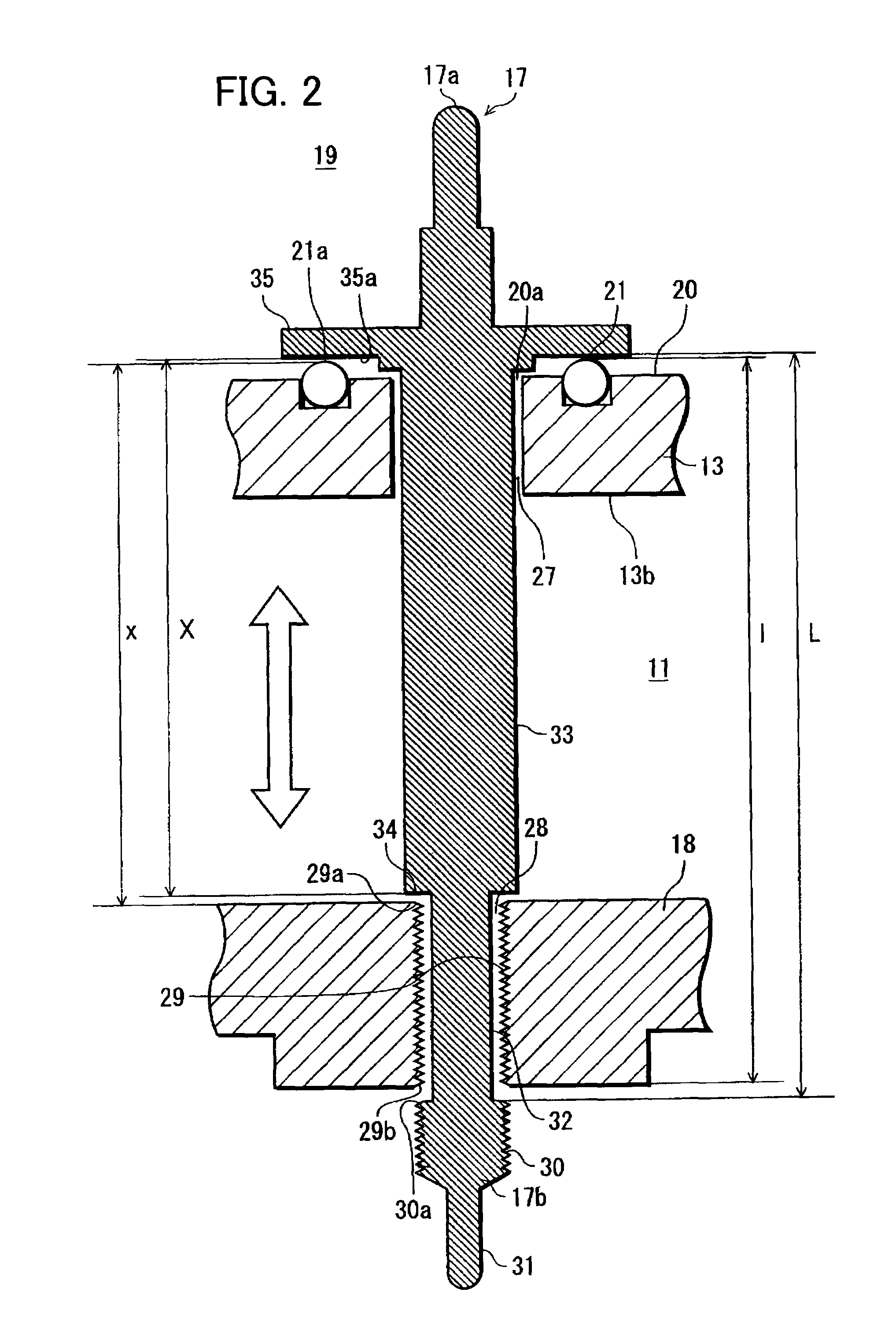
[0036]As shown in FIG. 1, the substrate processing apparatus 10 has a chamber 12 (processing chamber) having an internal space 11 (first space) in which a semiconductor wafer W (hereinafter referred to merely as a “wafer W”) is housed, a disk-shaped stage 13 (mounting stage) that is disposed in the internal space 11 and on which the wafer W is mounted, a stem 14 that is installed in a lower part of the chamber 12 in a standing manner and supports the stage 13, an enclosure 15 (cover member) that is disposed such as to face a surface 13a (substrate mounting surface) of the stage 13 on which the wafer W is mounted (hereinafter referred to as the “wafer mounting surface 13a”), a processing gas supply ...
PUM
| Property | Measurement | Unit |
|---|---|---|
| Diameter | aaaaa | aaaaa |
| Distance | aaaaa | aaaaa |
Abstract
Description
Claims
Application Information
 - Generate Ideas
- Intellectual Property
- Life Sciences
- Materials
- Tech Scout
- Unparalleled Data Quality
- Higher Quality Content
- 60% Fewer Hallucinations
Browse by: Latest US Patents, China's latest patents, Technical Efficacy Thesaurus, Application Domain, Technology Topic, Popular Technical Reports.
© 2025 PatSnap. All rights reserved.Legal|Privacy policy|Modern Slavery Act Transparency Statement|Sitemap|About US| Contact US: help@patsnap.com