Optical semiconductor device and method for manufacturing optical semiconductor device

Inactive Publication Date: 2008-09-04
KK TOSHIBA
View PDF8 Cites 35 Cited by
  • Summary
  • Abstract
  • Description
  • Claims
  • Application Information

AI Technical Summary

Benefits of technology

[0013]A second aspect of the embodiments of the present invention is to include, in a method for manufacturing the optical semiconductor device, forming a prevention member which prevents light from being incident upon the side surface of the concave portion of the base substrate; forming the base substrate by positioning the form

Problems solved by technology

However, the partial plating of the resin of the base substrate with silver increases the cost, because the plating requires a complicated manufacturing step such

Method used


Image

  • Optical semiconductor device and method for manufacturing optical semiconductor device
  • Optical semiconductor device and method for manufacturing optical semiconductor device
  • Optical semiconductor device and method for manufacturing optical semiconductor device

Examples


first embodiment

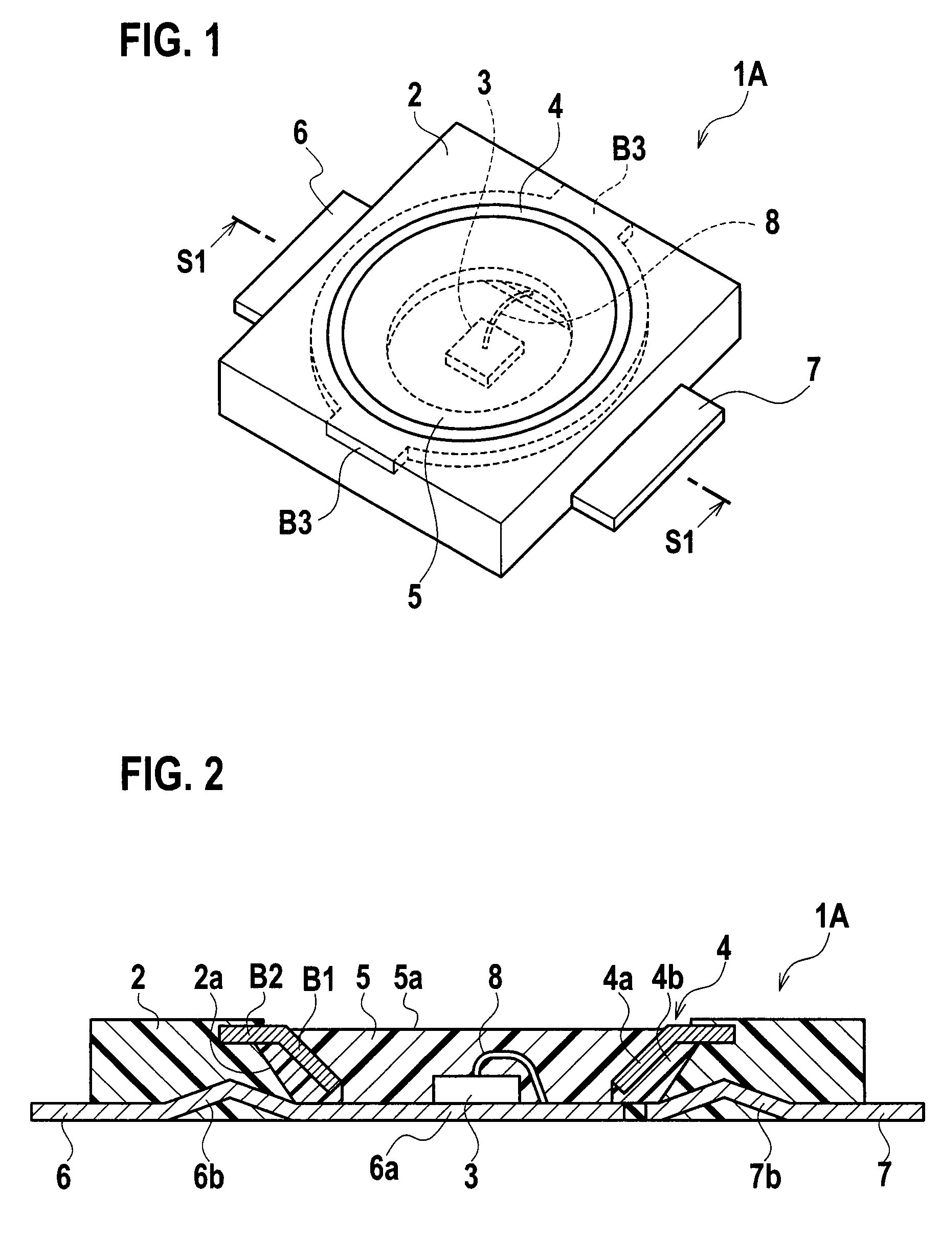
[0022]Descriptions of a first embodiment of the present invention will be given with reference to FIGS. 1 to 7.

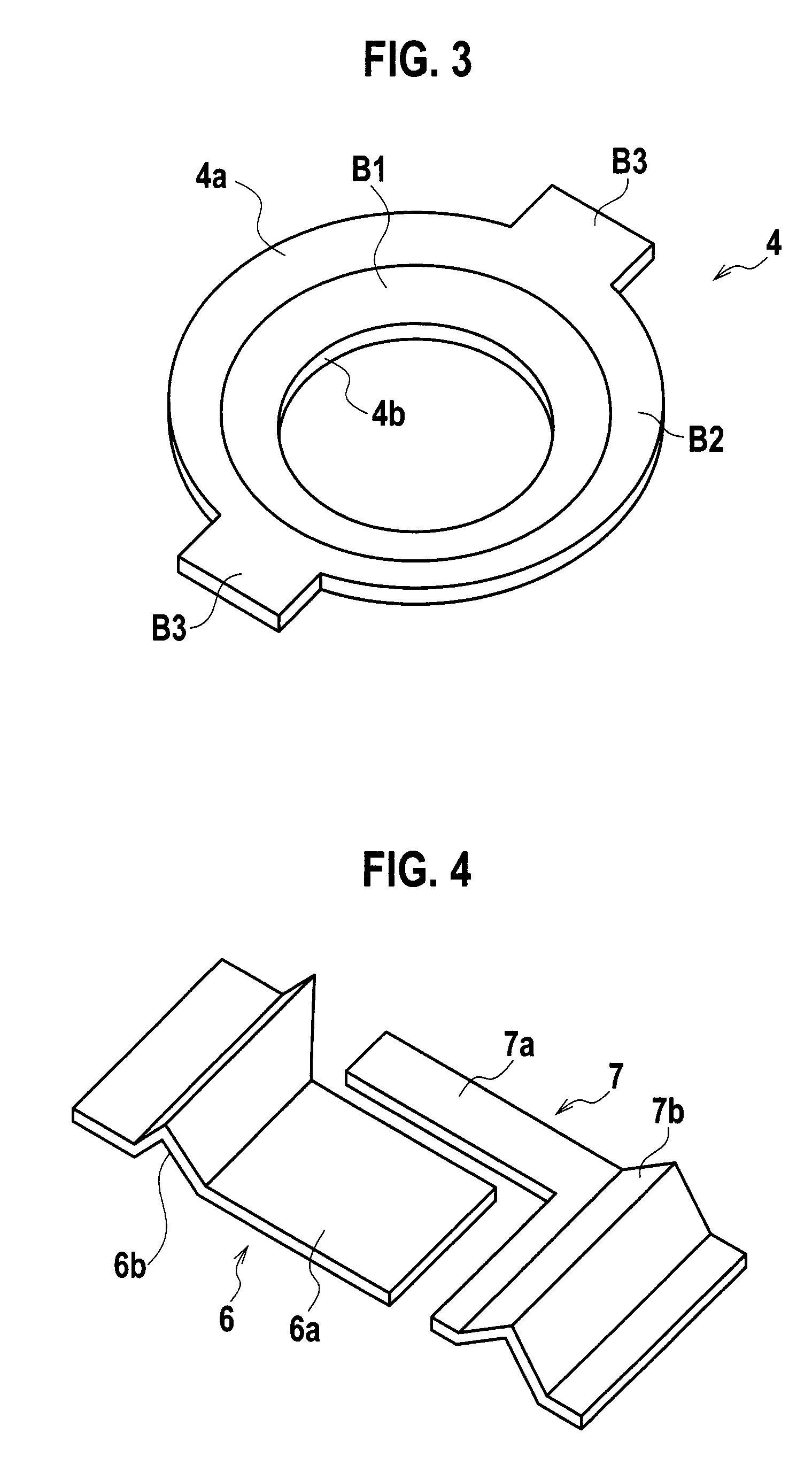
[0023]As shown in FIGS. 1 and 2, an optical semiconductor device 1A according to the first embodiment of the present invention includes a base substrate 2, a lighting-emitting element 3, a prevention member 4, a translucent member 5 and a pair of lead parts 6 and 7. The base substrate 2 has a concave portion 2a. The light-emitting element 3 is provided in the concave portion 2a and emits light. The prevention member 4 is provided to the base substrate 2 in a manner of covering a side (a side wall) of the concave portion 2a, and prevents light emitted by the light-emitting element 3 from being incident upon the side surface of the concave portion 2a. The translucent member 5 is provided in the concave portion 2a and seals the light-emitting element 3. The respective lead parts 6 and 7 are connected to the light-emitting element 3, and are extended from the bottom to the outs...

second embodiment

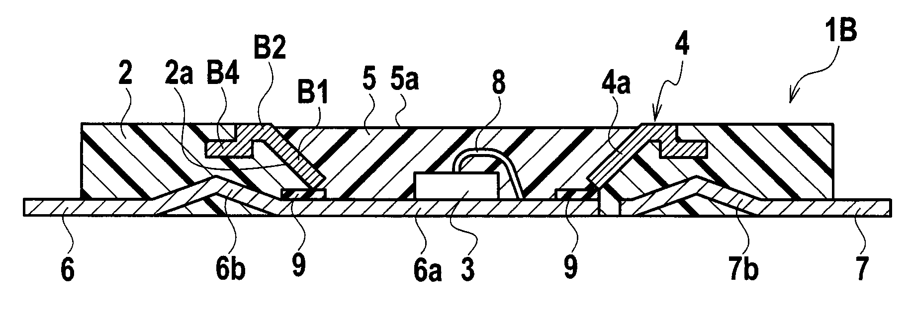
[0049]Descriptions of a second embodiment of the present invention will be given with reference to FIG. 8. In the second embodiment of the present invention, descriptions will be given of the parts which are different from the first embodiment. It should be noted that, in the second embodiment, the same symbols are attached to the same parts as those described in the first embodiment, and the descriptions thereof will be omitted.

[0050]As shown in FIG. 8, the prevention member 4 is configured of the reflection member 4a in an optical semiconductor device 1B according to the second embodiment of the present invention. Moreover, an insulation layer 9 having insulation properties is provided on the pair of lead parts 6 and 7. In addition, the marginal part B2 is provided with a step part B4.

[0051]The insulation layer 9 is provided in a position facing the reflection member 4a. In other words, the insulation layer 9 is provided in a circular form on the pair of lead parts 6 and 7 while f...


PUM


Abstract

An optical semiconductor device includes: a base substrate which has a concave portion; a light-emitting element which is provided in the concave portion, and which emits light; a prevention member which is provided to the base substrate in a manner of covering a side surface of the concave portion, and which prevents the light emitted by the light-emitting element from being incident on the side surface of the concave portion; and a translucent member which is provided in the concave portion, and which seals the light-emitting element.

Description

CROSS REFERENCE OF THE RELATED APPLICATION[0001]This application is based on and claims the benefit of priority from the prior Japanese Patent Application No. 2006-257740, filed on Sep. 22, 2006; the entire content of which are incorporated herein by reference.BACKGROUND OF THE INVENTION[0002]1. Field of the Invention[0003]The present invention relates to an optical semiconductor device having a light-emitting element and a method for manufacturing the optical semiconductor device.[0004]2. Description of the Related Art[0005]Optical semiconductor devices are used widely as light sources of various device, such as lighting and a display device, in different areas. As the optical semiconductor devices, proposed is an optical semiconductor device which produces white light and the like by combining light emitted by a light-emitting element and light emitted by a phosphor which is excited by the light emitted by a light-emitting element (refer to JP-A No. 2005-311136 (KOKAI), for exampl...

Claims


Application Information

Patent Timeline
IPC IPC(8): H01L33/00H01L21/00H01L33/54H01L33/56H01L33/62
CPCH01L33/486H01L33/60H01L33/62H01L2224/45144H01L2224/48247H01L2224/48257H01L2224/48091H01L2924/00014H01L2924/00H01L2924/181H01L2924/00012
Inventor TOMIOKA, TAIZO
Owner KK TOSHIBA
Why Eureka
Try Eureka