

Method and apparatus of electrical field assisted imprinting
- Summary
- Abstract
- Description
- Claims
- Application Information
AI Technical Summary
Benefits of technology
Problems solved by technology
Method used
Image

Examples
Embodiment Construction
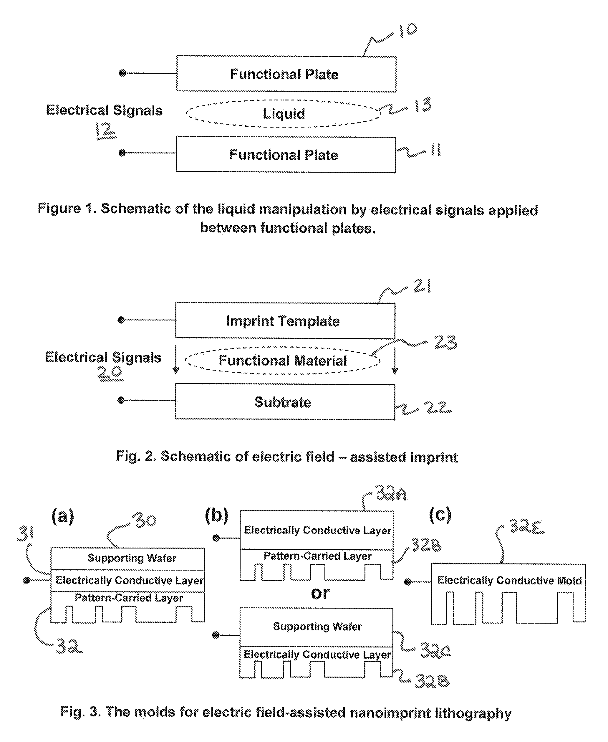
[0027]FIG. 1 illustrates—electric field-assisted liquid manipulation between functional plates 10, 11. Here, the electrical signals 12 (AC, DC, or arbitrary time-sequential signals) can induce various physical effects (electrowetting, dielectrophoresis, electrowetting-on-dieletric, electrostatic action, or other electrodynamic actions), which can be employed to control the transport or distribution of a liquid 13 or other material between functional plates or structured surfaces.
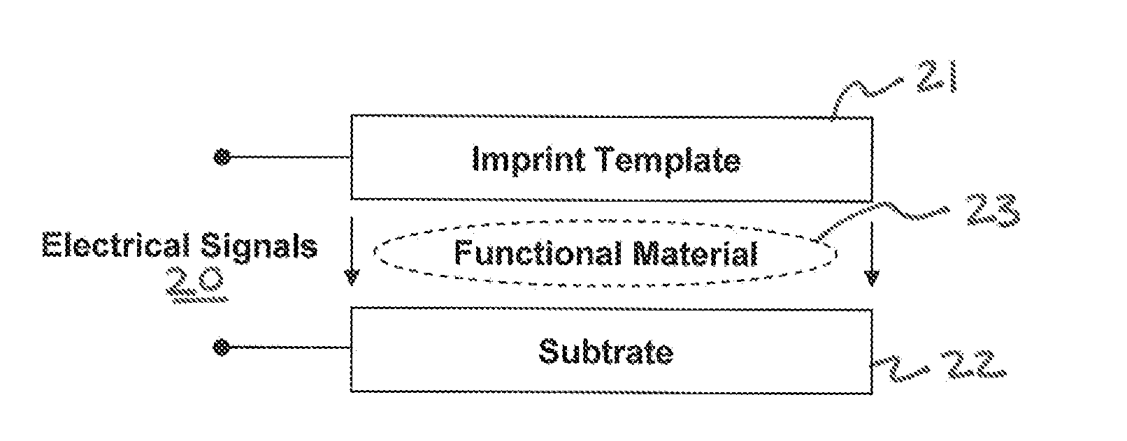
[0028]FIG. 2 shows a first embodiment, in which electrical signals 20 applied between an imprint template (mold) 21 and a substrate 22 induces the electrostatic force, which serves as the imprinting pressure to press the template into a layer of conformable functional material 23 (e.g. resist). After template separation, the structures are patterned into the functional material.
[0029]For electric field-assisted imprint, a typical imprint mold consists three parts (FIG. 3a): a supporting wafer 30, an electric...
PUM
| Property | Measurement | Unit |
|---|---|---|
| Electric field | aaaaa | aaaaa |
Abstract
Description
Claims
Application Information